- 您现在的位置:买卖IC网 > PDF目录98079 > SCANPSC100FDMQB (NATIONAL SEMICONDUCTOR CORP) SPECIALTY MICROPROCESSOR CIRCUIT, CDIP28 PDF资料下载
参数资料
| 型号: | SCANPSC100FDMQB |
| 厂商: | NATIONAL SEMICONDUCTOR CORP |
| 元件分类: | 微控制器/微处理器 |
| 英文描述: | SPECIALTY MICROPROCESSOR CIRCUIT, CDIP28 |
| 封装: | CERAMIC, DIP-28 |
| 文件页数: | 12/27页 |
| 文件大小: | 381K |
| 代理商: | SCANPSC100FDMQB |
第1页第2页第3页第4页第5页第6页第7页第8页第9页第10页第11页当前第12页第13页第14页第15页第16页第17页第18页第19页第20页第21页第22页第23页第24页第25页第26页第27页
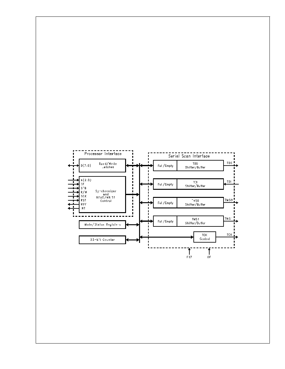
Chip Architecture
The ’PSC100 is designed to act together with a parallel bus
host as a serial test bus master. Parallel data is written by the
host to the ’PSC100, which serializes the data for application
to a serial test bus. Serial data returning from the target scan
chain(s) is placed on the processor port for parallel reads.
Several features are included in the ’PSC100 which make
scan test communication more convenient and efficient.
Figure 1 shows the major functional blocks of the ’PSC100
design. The Parallel Processor Interface (PPI) is an asyn-
chronous, 8-bit parallel interface which is used by the host
processor to write and read data. The PPI generates the
necessary internal data, address, and control signals to
complete internal write and read operations.
The Serial Scan Interface (SSI) consists of a bank of
double-buffered parallel/serial shift registers (i.e.,a2x8bit
FIFO), or Shifter/Buffers. The double buffering improves ef-
ficiency by allowing parallel writes or reads to/from one of the
two 8-bit FIFOs within the shifter/buffer while the other FIFO
is shifting data to/from the scan chain. Three Shifter/Buffers
are provided for outgoing serial data and one for incoming
serial data. Test Data Out (TDO) is for scanning out test data
while the two Test Mode Select signals (TMS0/1) are used to
provide user specific control data. Test Data In (TDI) re-
ceives serial data from the scan chain. A local control block
is associated with each Shifter/Buffer to provide shift and
load control as well as providing full or empty status. The SSI
also provides Test Clock (TCK) Control. TCK is stopped and
started depending on the status of the Shifter/Buffers or the
32-bit Counter. By stopping and starting TCK, scan opera-
tions will proceed only when the enabled Shifter/Buffers are
ready to send and/or receive serial data.
The 32-bit Counter (CNT32) is a count-down binary counter
included to assist in controlling the SSI. The initial state of
CNT32 is loaded from the parallel port with four consecutive
writes to its address. When enabled, CNT32 is used to
program the number of TCKs applied by the SSI to the
boundary scan chain(s). The value of CNT32 can also be
used to generate interrupts (i.e., when CNT32 reaches ter-
minal count) and to trigger ’PSC100 features, such as, Auto
TMS High (discussed later within this datasheet).
The Mode and Status Registers are used to control and
observe the operation of the SSI and CNT32. Each of the
Shifter/Buffers and CNT32 have an associated mode bit
which enables it for participation in on-going operations.
Status bits can be used for polling operations.
10032502
FIGURE 1. ’PSC100 Block Diagram
SCANPSC100F
Embedded
www.national.com
2
相关PDF资料 |
PDF描述 |
|---|---|
| SCANPSC100FLMQB | SPECIALTY MICROPROCESSOR CIRCUIT, CQCC28 |
| SCB68172C2F28 | VME BUS CONTROLLER, CDIP28 |
| SCC2691AC1D24 | 1 CHANNEL(S), 38.4K bps, SERIAL COMM CONTROLLER, PDSO24 |
| SCC2691AE1A28 | 1 CHANNEL(S), 38.4K bps, SERIAL COMM CONTROLLER, PQCC28 |
| SCC2692AC1A44-T | 2 CHANNEL(S), 1M bps, SERIAL COMM CONTROLLER, PQCC44 |
相关代理商/技术参数 |
参数描述 |
|---|---|
| SCANPSC100FLMQB | 制造商:Texas Instruments 功能描述: |
| SCANPSC100FSC | 功能描述:接口 - 专用 Emb Boun Scan Cont RoHS:否 制造商:Texas Instruments 产品类型:1080p60 Image Sensor Receiver 工作电源电压:1.8 V 电源电流:89 mA 最大功率耗散: 最大工作温度:+ 85 C 安装风格:SMD/SMT 封装 / 箱体:BGA-59 |
| SCANPSC100FSCX | 功能描述:接口 - 专用 Emb Boun Scan Cont RoHS:否 制造商:Texas Instruments 产品类型:1080p60 Image Sensor Receiver 工作电源电压:1.8 V 电源电流:89 mA 最大功率耗散: 最大工作温度:+ 85 C 安装风格:SMD/SMT 封装 / 箱体:BGA-59 |
| SCANPSC110 | 制造商:NSC 制造商全称:National Semiconductor 功能描述:SCAN Bridge Hierarchical and Multidrop Addressable JTAG Port (IEEE1149.1 System Test Support) |
| SCANPSC110_ZFC3026B WAF | 制造商:Fairchild Semiconductor Corporation 功能描述: |
发布紧急采购,3分钟左右您将得到回复。