- 您现在的位置:买卖IC网 > PDF目录9967 > SI5110-H-GL (Silicon Laboratories Inc)IC TXRX SONET/SDH LP HS 99LFBGA PDF资料下载
参数资料
| 型号: | SI5110-H-GL |
| 厂商: | Silicon Laboratories Inc |
| 文件页数: | 7/36页 |
| 文件大小: | 0K |
| 描述: | IC TXRX SONET/SDH LP HS 99LFBGA |
| 标准包装: | 168 |
| 系列: | SiPHY™ |
| 类型: | 收发器 |
| 驱动器/接收器数: | 1/1 |
| 规程: | SONET/SDH |
| 电源电压: | 1.71 V ~ 1.89 V |
| 安装类型: | 表面贴装 |
| 封装/外壳: | 99-LBGA |
| 供应商设备封装: | 99-BGA(11x11) |
| 包装: | 托盘 |
第1页第2页第3页第4页第5页第6页当前第7页第8页第9页第10页第11页第12页第13页第14页第15页第16页第17页第18页第19页第20页第21页第22页第23页第24页第25页第26页第27页第28页第29页第30页第31页第32页第33页第34页第35页第36页
Si5110
Rev. 1.5
15
reacquisition, the recovered clock frequency (RXCLK1
and RXCLK2) drifts over a range of approximately
±1000 ppm relative to the supplied reference clock
unless LTR is asserted. The RXLOL output remains
asserted until the frequency of the (divided) recovered
clock differs from the reference clock frequency by less
than the amount specified in Table 5 on page 9.
The RXLOL output will be asserted automatically if a
valid reference clock is not detected.
The RXLOL output will also be asserted whenever the
loss of signal alarm (LOS) is active, provided that the
LTR input is set high (i.e., provided that the device is not
configured for Lock-to-Reference mode).
5.3.3. Lock-to-Reference
The lock-to-reference (LTR) input can be utilized to
ensure the presence of a stable output clock during a
loss-of-signal alarm (LOS). When LTR is asserted, the
CDR is prevented from phase locking to the data signal
and the CDR locks the RXCLKOUT1 and RXCLKOUT2
outputs to the reference clock. In typical applications,
the LOS output is tied to the LTR input to force a stable
output clock during a loss-of-signal condition.
5.4. Deserialization
The Si5110 uses a 1:4 demultiplexer to deserialize the
high-speed input. The deserialized data is output on a
4-bit parallel data bus, RXDOUT[3:0], aligned with the
rising edge of RXCLK1.
5.4.1. Serial Input to Parallel Output Relationship
The Si5110 provides the capability to select the order in
which the received serial data is mapped to the parallel
output bus RXDOUT[3:0]. The mapping of the receive
bits to the output data word is controlled by the
RXMSBSEL input. When RXMSBSEL is set low, the
first bit received is output on RXDOUT0, and the
following bits are output in order on RXDOUT1 through
RXDOUT3. When RXMSBSEL is set high, the first bit
received is output on RXDOUT3, and the following bits
are output in order on RXDOUT2 through RXDOUT0.
5.5. Voltage Reference Output
The Si5110 provides an output voltage reference that
can be used by external circuitry to set the LOS
threshold, slicing level, or sampling phase adjustment
input voltage levels. One possible implementation uses
a resistor divider to set the control voltage for the
LOSLVL,
SLICELVL,
or
PHASEADJ
inputs.
An
alternative is the use of digital-to-analog converters
(DACs) to set the control voltages. Using this approach,
VREF is used to set the range of the DAC outputs. The
voltage on the VREF output is nominally 1.25 V.
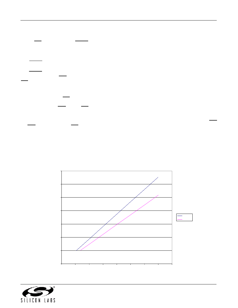
Figure 4. Typical LOSLVL Transfer Curve, Absolute Slice Mode (SLICEMODE = 0)
0
50
100
150
200
250
300
350
0
0.05
0.1
0.15
0.2
0.25
0.3
0.35
0.4
LOSLV (V)
V
LOS
(mV)
Assert
DeAssert
V L
O
S
=
.9
58
LO
SL
VL
V LO
S
= .
76
2 L
OS
LV
L
相关PDF资料 |
PDF描述 |
|---|---|
| MAX11206EEE+T | IC ADC 20BIT 16QSOP |
| GTC06A-20-18P | CONN PLUG 9POS STRAIGHT W/PINS |
| IDT723634L15PF8 | IC FIFO SYNC 512X36X2 128QFP |
| MAX11626EEE+T | IC ADC 12BIT 4CH 16QSOP |
| IDT72815LB25BG8 | IC FIFO SYNC DUAL 512X18 121BGA |
相关代理商/技术参数 |
参数描述 |
|---|---|
| SI5110-H-XL4 | 制造商:Silicon Laboratories Inc 功能描述:OC-48 TRANSCEIVER, LIA, CDR, 4:1 MUX, 1:4 DEMUX - Rail/Tube |
| SI5110-H-ZL3 | 制造商:Silicon Laboratories Inc 功能描述:OC-48 TRANSCEIVER, LIA, CDR, 4:1 MUX, 1:4 DEMUX - Rail/Tube |
| SI511BBA200M000BAGR | 制造商:Silicon Laboratories Inc 功能描述:SLLSI511BBA200M000BAGR OSC (200MHZ) |
| SI51210 | 制造商:SILABS 制造商全称:SILABS 功能描述:TWO OUTPUTS FACTORY PROGRAMMABLE CLOCK GENERATOR |
| Si51210-A01AFM | 功能描述:时钟发生器及支持产品 6 TDFN microClockgen SL Clock RoHS:否 制造商:Silicon Labs 类型:Clock Generators 最大输入频率:14.318 MHz 最大输出频率:166 MHz 输出端数量:16 占空比 - 最大:55 % 工作电源电压:3.3 V 工作电源电流:1 mA 最大工作温度:+ 85 C 安装风格:SMD/SMT 封装 / 箱体:QFN-56 |
发布紧急采购,3分钟左右您将得到回复。