- 您现在的位置:买卖IC网 > PDF目录2108 > SI5320-H-BL (Silicon Laboratories Inc)IC CLOCK MULT SONET/SDH 63-PBGA PDF资料下载
参数资料
| 型号: | SI5320-H-BL |
| 厂商: | Silicon Laboratories Inc |
| 文件页数: | 10/34页 |
| 文件大小: | 0K |
| 描述: | IC CLOCK MULT SONET/SDH 63-PBGA |
| 标准包装: | 260 |
| 系列: | DSPLL® |
| 类型: | 时钟乘法器 |
| PLL: | 是 |
| 输入: | LVTTL |
| 输出: | CML |
| 电路数: | 1 |
| 比率 - 输入:输出: | 1:1 |
| 差分 - 输入:输出: | 是/是 |
| 频率 - 最大: | 693MHz |
| 除法器/乘法器: | 是/是 |
| 电源电压: | 3.135 V ~ 3.465 V |
| 工作温度: | -20°C ~ 85°C |
| 安装类型: | 表面贴装 |
| 封装/外壳: | 63-LBGA |
| 供应商设备封装: | 63-PBGA(9x9) |
| 包装: | 托盘 |
第1页第2页第3页第4页第5页第6页第7页第8页第9页当前第10页第11页第12页第13页第14页第15页第16页第17页第18页第19页第20页第21页第22页第23页第24页第25页第26页第27页第28页第29页第30页第31页第32页第33页第34页
Si5320
18
Rev. 2.5
minimizes the output clock jitter variation from board to
board, providing more consistent system level jitter
performance.
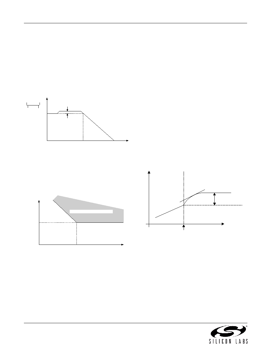
The jitter transfer characteristic is a function of the
BWSEL[1:0] setting. (See Table 7.) Lower bandwidth
selection settings result in more jitter attenuation of the
incoming clock but may result in higher jitter generation.
Table 4 on page 9 gives the 3 dB bandwidth and
peaking values for specified BWSEL settings. Figure 6
shows the jitter transfer curve mask.
Figure 6. PLL Jitter Transfer Mask/Template
2.3.3. Jitter Tolerance
Jitter tolerance for the Si5320 is defined as the
maximum peak-to-peak sinusoidal jitter that can be
present on the incoming clock. The tolerance is a
function of the jitter frequency, because tolerance
improves for lower input jitter frequency. See Figure 7.
Figure 7. Jitter Tolerance Mask/Template
2.4. Digital Hold of the PLL
When no valid input clock is available, the Si5320
digitally holds the internal oscillator to its last frequency
value. This provides a stable clock to the system until an
input clock is again valid. This clock maintains very
stable operation in the presence of constant voltage and
temperature. The frequency accuracy specifications for
digital hold mode are given in Table 4 on page 9.
2.5. Hitless Recovery from Digital Hold
When the Si5320 device is locked to a valid input clock,
a loss of the input clock causes the device to
automatically switch to digital hold mode. When the
input clock signal returns, the device performs a
“hitless” transition from digital hold mode back to the
selected input clock. That is, the device performs
“phase build-out” to absorb the phase difference
between the internal VCO clock operating in digital hold
mode and the new/returned input clock. The maximum
phase step size seen at the clock output during this
transition and the maximum slope for this phase step
are given in Table 4 on page 9.
This feature can be disabled by asserting the
FXDDELAY pin. When the FXDDELAY pin is high, the
output clock is phase and frequency locked with a
known
phase
relationship
to
the
input
clock.
Consequently, any abrupt phase change on the input
clock propagates through the device, and the output
slews at the selected loop bandwidth until the original
phase relationship is restored.
Note: When the DBLBW is asserted, hitless recovery must
also be disabled by driving FXDDELAY high for proper
operation.
Figure 8. Recovery from Digital Hold
2.6. Loss-of-Signal Alarm
The Si5320 has loss-of-signal (LOS) circuitry that
constantly monitors the CLKIN input clock for missing
pulses. The LOS circuitry sets a LOS output alarm
signal when missing pulses are detected.
The LOS circuitry operates as follows. Regardless of
the selected input clock frequency range, the LOS
circuitry divides down the input clock into the 19 MHz
range. The LOS circuitry then over-samples this
divided-down input clock to search for extended periods
of time without input clock transitions. If the LOS
Jitter
Transfer
0 dB
F
BW
f
Jitter
Peaking
–20 dB/dec.
Jitter Out
Jitter In
(s)
Input
Jitter
Amplitude
10 ns
F
BW
–20 dB/dec.
f
Jitter In
Excessive Input Jitter Range
Recovery from
digital hold
m
PT
t
PT_MTIE
相关PDF资料 |
PDF描述 |
|---|---|
| SI5320-H-GL | IC CLOCK MULT SONET/SDH 63LFBGA |
| SI5321-G-BC | IC PREC CLOCK MULTIPLIER 63CBGA |
| SI5321-H-BL | IC CLOCK MULT SONET/SDH 63-PBGA |
| SI5322-B-GM | IC PREC CLOCK MULTIPLIER 36QFN |
| SI5323-B-GM | IC MULTIPLIER/ATTENUATOR 36QFN |
相关代理商/技术参数 |
参数描述 |
|---|---|
| Si5320-H-GL | 功能描述:时钟发生器及支持产品 SONET/SDH Precisn Clock Multiplr RoHS:否 制造商:Silicon Labs 类型:Clock Generators 最大输入频率:14.318 MHz 最大输出频率:166 MHz 输出端数量:16 占空比 - 最大:55 % 工作电源电压:3.3 V 工作电源电流:1 mA 最大工作温度:+ 85 C 安装风格:SMD/SMT 封装 / 箱体:QFN-56 |
| SI5320-X-BC | 制造商:未知厂家 制造商全称:未知厂家 功能描述:SONET/SDH PRECISION CLOCK MULTIPLIER IC |
| SI5321 | 制造商:未知厂家 制造商全称:未知厂家 功能描述:SONET/SDH PRECISION CLOCK MULTIPLIER IC |
| SI5321-EVB | 功能描述:时钟和定时器开发工具 G.709FEC & 66/64Sc 19-2.5GHz Output RoHS:否 制造商:Texas Instruments 产品:Evaluation Modules 类型:Clock Conditioners 工具用于评估:LMK04100B 频率:122.8 MHz 工作电源电压:3.3 V |
| SI5321-F-BC | 功能描述:时钟合成器/抖动清除器 FOR NEW DESIGNS RoHS:否 制造商:Skyworks Solutions, Inc. 输出端数量: 输出电平: 最大输出频率: 输入电平: 最大输入频率:6.1 GHz 电源电压-最大:3.3 V 电源电压-最小:2.7 V 封装 / 箱体:TSSOP-28 封装:Reel |
发布紧急采购,3分钟左右您将得到回复。