- 您现在的位置:买卖IC网 > PDF目录2108 > SI5320-H-BL (Silicon Laboratories Inc)IC CLOCK MULT SONET/SDH 63-PBGA PDF资料下载
参数资料
| 型号: | SI5320-H-BL |
| 厂商: | Silicon Laboratories Inc |
| 文件页数: | 11/34页 |
| 文件大小: | 0K |
| 描述: | IC CLOCK MULT SONET/SDH 63-PBGA |
| 标准包装: | 260 |
| 系列: | DSPLL® |
| 类型: | 时钟乘法器 |
| PLL: | 是 |
| 输入: | LVTTL |
| 输出: | CML |
| 电路数: | 1 |
| 比率 - 输入:输出: | 1:1 |
| 差分 - 输入:输出: | 是/是 |
| 频率 - 最大: | 693MHz |
| 除法器/乘法器: | 是/是 |
| 电源电压: | 3.135 V ~ 3.465 V |
| 工作温度: | -20°C ~ 85°C |
| 安装类型: | 表面贴装 |
| 封装/外壳: | 63-LBGA |
| 供应商设备封装: | 63-PBGA(9x9) |
| 包装: | 托盘 |
第1页第2页第3页第4页第5页第6页第7页第8页第9页第10页当前第11页第12页第13页第14页第15页第16页第17页第18页第19页第20页第21页第22页第23页第24页第25页第26页第27页第28页第29页第30页第31页第32页第33页第34页
Si5320
Rev. 2.5
19
circuitry detects four consecutive samples of the
divided-down input clock that are the same state (i.e.,
1111 or 0000), a LOS condition is declared, the Si5320
goes into digital hold mode, and the LOS output alarm
signal is set high. The LOS sampling circuitry runs at a
frequency of fO_622/8, where fO_622 is the output clock
frequency when the FRQSEL[1:0] pins are set to 11.
Table 3 on page 7 lists the minimum and maximum
transitionless time periods required for declaring a LOS
on the input clock (tLOS).
Once the LOS alarm is asserted, it is held high until the
input clock is validated over a time period designated by
the VALTIME pin. When VALTIME is low, the validation
time period is about 100 ms. When VALTIME is high,
the validation time period is about 13 s. If another LOS
condition is detected on the input clock during the
validation time (i.e., if another set of 1111 or 0000
samples are detected), the LOS alarm remains
asserted, and the validation time starts over. When the
LOS alarm is finally released, the Si5320 exits digital
hold mode and locks to the input clock. The LOS alarm
is automatically set high at power-on and at every low-
to-high transition of the RSTN/CAL pin. In these cases,
the Si5320 undergoes a self-calibration before releasing
the LOS alarm and locking to the input clock.
The Si5320 also provides an output indicating the digital
hold status of the device, DH_ACTV. The Si5320 only
enters the digital hold mode upon the loss of the input
clock. When this occurs, the LOS alarm will also be
active. Therefore, applications that require monitoring of
the status of the Si5320 need only monitor the
CAL_ACTV and either the LOS or DH_ACTV outputs to
know the state of the device.
2.7. Reset
The Si5320 provides a Reset/Calibration pin, RSTN/
CAL, which resets the device and disables the outputs.
When the RSTN/CAL pin is driven low, the internal
circuitry enters into the reset mode, and all LVTTL
outputs are forced into a high-impedance state. Also,
the CLKOUT+ and CLKOUT– pins are forced to a
nominal CML logic LOW and HIGH respectively (See
Figure 9). This feature is useful for in-circuit test
applications. A low-to-high transition on RSTN/CAL
initializes all digital logic to a known condition and
initiates self-calibration of the DSPLL. Upon completion
of self-calibration, the DSPLL begins to lock to the clock
input signal.
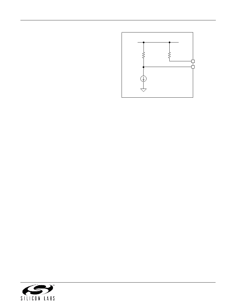
Figure 9. CLKOUT± Equivalent Circuit, RSTN/
CAL asserted LOW
2.8. PLL Self-Calibration
The Si5320 achieves optimal jitter performance by
using self-calibration circuitry to set the VCO center
frequency and loop gain parameters within the DSPLL.
Internal circuitry generates self calibration automatically
on powerup or after a loss of power condition. Self-
calibration can also be manually initiated by a low-to-
high transition on the RSTN/CAL input.
A self-calibration should be initiated after changing the
state of the FEC[1:0] inputs.
Whether manually initiated or automatically initiated at
powerup, the self-calibration process requires the
presence of a valid input clock.
If the self-calibration is initiated without a valid clock
present, the device waits for a valid clock before
completing the self-calibration. The Si5320 clock output
is set to the lower end of the operating frequency range
while the device is waiting for a valid clock. After the
clock input is validated, the calibration process runs to
completion; the device locks to the clock input, and the
clock output shifts to its target frequency. Subsequent
losses of the input clock signal do not require re-
calibration. If the clock input is lost following self-
calibration, the device enters digital hold mode. When
the input clock returns, the device re-locks to the input
clock without performing a self-calibration. During the
calibration process, the output clock frequency is
indeterminate and may jump as high as 5% above the
final locked value.
100
Ω
VDD 2.5 V
100
Ω
CLKOUT–
CLKOUT+
15 mA
相关PDF资料 |
PDF描述 |
|---|---|
| SI5320-H-GL | IC CLOCK MULT SONET/SDH 63LFBGA |
| SI5321-G-BC | IC PREC CLOCK MULTIPLIER 63CBGA |
| SI5321-H-BL | IC CLOCK MULT SONET/SDH 63-PBGA |
| SI5322-B-GM | IC PREC CLOCK MULTIPLIER 36QFN |
| SI5323-B-GM | IC MULTIPLIER/ATTENUATOR 36QFN |
相关代理商/技术参数 |
参数描述 |
|---|---|
| Si5320-H-GL | 功能描述:时钟发生器及支持产品 SONET/SDH Precisn Clock Multiplr RoHS:否 制造商:Silicon Labs 类型:Clock Generators 最大输入频率:14.318 MHz 最大输出频率:166 MHz 输出端数量:16 占空比 - 最大:55 % 工作电源电压:3.3 V 工作电源电流:1 mA 最大工作温度:+ 85 C 安装风格:SMD/SMT 封装 / 箱体:QFN-56 |
| SI5320-X-BC | 制造商:未知厂家 制造商全称:未知厂家 功能描述:SONET/SDH PRECISION CLOCK MULTIPLIER IC |
| SI5321 | 制造商:未知厂家 制造商全称:未知厂家 功能描述:SONET/SDH PRECISION CLOCK MULTIPLIER IC |
| SI5321-EVB | 功能描述:时钟和定时器开发工具 G.709FEC & 66/64Sc 19-2.5GHz Output RoHS:否 制造商:Texas Instruments 产品:Evaluation Modules 类型:Clock Conditioners 工具用于评估:LMK04100B 频率:122.8 MHz 工作电源电压:3.3 V |
| SI5321-F-BC | 功能描述:时钟合成器/抖动清除器 FOR NEW DESIGNS RoHS:否 制造商:Skyworks Solutions, Inc. 输出端数量: 输出电平: 最大输出频率: 输入电平: 最大输入频率:6.1 GHz 电源电压-最大:3.3 V 电源电压-最小:2.7 V 封装 / 箱体:TSSOP-28 封装:Reel |
发布紧急采购,3分钟左右您将得到回复。