- 您现在的位置:买卖IC网 > PDF目录16791 > SI5338-EVB (Silicon Laboratories Inc)BOARD EVALUATION SI5338 PDF资料下载
参数资料
| 型号: | SI5338-EVB |
| 厂商: | Silicon Laboratories Inc |
| 文件页数: | 16/44页 |
| 文件大小: | 0K |
| 描述: | BOARD EVALUATION SI5338 |
| 标准包装: | 1 |
| 主要目的: | 计时,时钟发生器 |
| 嵌入式: | 否 |
| 已用 IC / 零件: | Si5338 |
| 主要属性: | LVPECL/LVDS:160 kHz 至 700 MHz,<1 ps RMS 标准抖动,零 ppm 频率错误 |
| 次要属性: | 基于 USB 的 GUI,用于编程,I2C/SMBus 兼容接口,1.8、2.5 或 3.3 V |
| 已供物品: | 板,线缆,CD,样品 |
| 产品目录页面: | 628 (CN2011-ZH PDF) |
| 相关产品: | 336-1555-5-ND - IC CLK GEN QUAD 200MHZ 24-QFN 336-1554-5-ND - IC CLK GEN QUAD 350MHZ 24-QFN 336-1553-5-ND - IC CLK GEN QUAD 700MHZ 24-QFN |
| 其它名称: | 336-1556 |
第1页第2页第3页第4页第5页第6页第7页第8页第9页第10页第11页第12页第13页第14页第15页当前第16页第17页第18页第19页第20页第21页第22页第23页第24页第25页第26页第27页第28页第29页第30页第31页第32页第33页第34页第35页第36页第37页第38页第39页第40页第41页第42页第43页第44页
Si5338
Rev. 1.3
23
3.5.4. Writing a Custom Configuration to NVM
An alternative to ordering an Si5338 with a custom NVM
configuration is to use the field programming kit
(Si5338/56-PROG-EVB) to write directly to the NVM of
a “blank” Si5338. Since NVM is an OTP memory, it can
only be written once. The default configuration can be
reconfigured by writing to RAM through the I2C interface
3.6. Status Indicators
A logic-high interrupt pin (INTR) is available to indicate
a loss of signal (LOS) condition, a PLL loss of lock
(PLL_LOL) condition, or that the PLL is in process of
acquiring lock (SYS_CAL). PLL_LOL is held high when
the input frequency drifts beyond the PLL tracking
range. It is held low during all other times and during a
POR or soft_reset. SYS_CAL is held high during a POR
or SOFT reset so that no chattering occurs during the
locking process. As shown in Figure 10, a status
register at address 218 is available to help identify the
exact event that caused the interrupt pin to become
active. Register 247 is the sticky version of Register
218, and Register 6 is the interrupt mask for Register
218.
Figure 10. Status Register
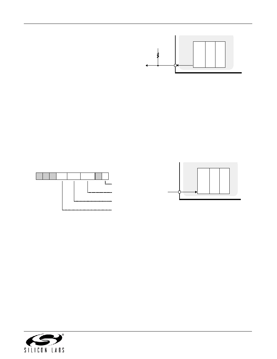
Figure 11 shows a typical connection with the required
pull-up resistor to VDD.
3.6.1. Using the INTR Pin in Systems with I2C
The INTR output pin is not latched and thus it should not
be a polled input to an MCU but an edge-triggered
interrupt. An MCU can process an interrupt event by
reading the sticky register 247 to see what event
caused the interrupt. The same register can be cleared
by writing zeros to the bits that were set. Individual
interrupt bits can be masked by register 6[4:0].
3.6.2. Using the INTR Pin in Systems without I2C
The INTR pin also provides a useful function in systems
that require a pin-controlled fault indicator. Pre-setting
the interrupt mask register allows the INTR pin to
become an indicator for a specific event, such as LOS
and/or LOL. Therefore, the INTR pin can be used to
indicate a single fault event or even multiple events.
Figure 11. INTR Pin with Required Pull-Up
3.7. Output Enable
There are two methods of enabling and disabling the
output drivers: Pin control, and I2C control.
3.7.1. Enabling Outputs Using Pin Control
The Si5338K/L/M devices provide an Output Enable pin
(OEB) as shown in Figure 12. Pulling this pin high will
turn all outputs off. The state of the individual drivers
when turned off is controllable. If an individual output is
set to always on, then the OEB pin will not have an
effect on that driver. Drive state options and always on
are explained in “3.7.2. Enabling Outputs through the
Figure 12. Output Enable Pin (Si5338K/L/M)
3.7.2. Enabling Outputs through the I2C Interface
Output enable can be controlled through the I2C
interface. As shown in Figure 13, register 230[3:0]
allows control of each individual output driver. Register
230[4] controls all drivers at once. When register 230[4]
is set to disable all outputs, the individual output
enables will have no effect. Registers 110[7:6], 114[7:6],
118[7:6], and 112[7:6] control the output disabled state
as tri-state, low, high, or always on. If always on is set,
that output will always be on regardless of any other
register or chip state. In addition, the always on mode
must be selected for an output that is fed back in a Zero
Delay application.
218
System Calibration
(Lock Acquisition)
Sys
Cal
0
PLL_LOL
1
2
3
4
5
6
7
Loss Of Signal
Clock Input
Loss Of Signal
Feedback Input
Loss Of Lock
LOS_FDBK LOS_CLKIN
INTR
VDD
1k
Control
NVM
(OTP)
Control & Memory
RAM
OEB
Control
NVM
(OTP)
Control & Memory
RAM
0 = Enabled
1 = Disabled
相关PDF资料 |
PDF描述 |
|---|---|
| H3AAH-2606G | IDC CABLE - HSC26H/AE26G/HSC26H |
| 0982660138 | CBL 12POS 0.5MM JMPR TYPE D 1' |
| 0982661084 | CBL 37POS 0.5MM JMPR TYPE D 6" |
| HMC08DRTH | CONN EDGECARD 16POS DIP .100 SLD |
| EBC43DCSD-S288 | CONN EDGECARD 86POS .100 EXTEND |
相关代理商/技术参数 |
参数描述 |
|---|---|
| SI5338F-A01839-GM | 制造商:Silicon Laboratories Inc 功能描述:CLOCK - Bulk |
| SI5338F-A01839-GMR | 制造商:Silicon Laboratories Inc 功能描述:CLOCK - Tape and Reel |
| Si5338F-A-GM | 功能描述:时钟发生器及支持产品 I2C-PRGRMBL clock generatr 0.16-200MHz RoHS:否 制造商:Silicon Labs 类型:Clock Generators 最大输入频率:14.318 MHz 最大输出频率:166 MHz 输出端数量:16 占空比 - 最大:55 % 工作电源电压:3.3 V 工作电源电流:1 mA 最大工作温度:+ 85 C 安装风格:SMD/SMT 封装 / 箱体:QFN-56 |
| SI5338F-A-GMR | 功能描述:时钟发生器及支持产品 I2C-Program Clk Gen 0.16-200MHz Pin-Ctrl RoHS:否 制造商:Silicon Labs 类型:Clock Generators 最大输入频率:14.318 MHz 最大输出频率:166 MHz 输出端数量:16 占空比 - 最大:55 % 工作电源电压:3.3 V 工作电源电流:1 mA 最大工作温度:+ 85 C 安装风格:SMD/SMT 封装 / 箱体:QFN-56 |
| Si5338F-B-GM | 功能描述:时钟发生器及支持产品 I2C-PRGRMBL clock generatr 0.16-200MHz RoHS:否 制造商:Silicon Labs 类型:Clock Generators 最大输入频率:14.318 MHz 最大输出频率:166 MHz 输出端数量:16 占空比 - 最大:55 % 工作电源电压:3.3 V 工作电源电流:1 mA 最大工作温度:+ 85 C 安装风格:SMD/SMT 封装 / 箱体:QFN-56 |
发布紧急采购,3分钟左右您将得到回复。