- 您现在的位置:买卖IC网 > PDF目录16791 > SI5338-EVB (Silicon Laboratories Inc)BOARD EVALUATION SI5338 PDF资料下载
参数资料
| 型号: | SI5338-EVB |
| 厂商: | Silicon Laboratories Inc |
| 文件页数: | 24/44页 |
| 文件大小: | 0K |
| 描述: | BOARD EVALUATION SI5338 |
| 标准包装: | 1 |
| 主要目的: | 计时,时钟发生器 |
| 嵌入式: | 否 |
| 已用 IC / 零件: | Si5338 |
| 主要属性: | LVPECL/LVDS:160 kHz 至 700 MHz,<1 ps RMS 标准抖动,零 ppm 频率错误 |
| 次要属性: | 基于 USB 的 GUI,用于编程,I2C/SMBus 兼容接口,1.8、2.5 或 3.3 V |
| 已供物品: | 板,线缆,CD,样品 |
| 产品目录页面: | 628 (CN2011-ZH PDF) |
| 相关产品: | 336-1555-5-ND - IC CLK GEN QUAD 200MHZ 24-QFN 336-1554-5-ND - IC CLK GEN QUAD 350MHZ 24-QFN 336-1553-5-ND - IC CLK GEN QUAD 700MHZ 24-QFN |
| 其它名称: | 336-1556 |
第1页第2页第3页第4页第5页第6页第7页第8页第9页第10页第11页第12页第13页第14页第15页第16页第17页第18页第19页第20页第21页第22页第23页当前第24页第25页第26页第27页第28页第29页第30页第31页第32页第33页第34页第35页第36页第37页第38页第39页第40页第41页第42页第43页第44页
Si5338
30
Rev. 1.3
5. I2C Interface
Configuration and operation of the Si5338 is controlled
by reading and writing to the RAM space using the I2C
interface. The device operates in slave mode with 7-bit
addressing
and
can
operate
in
Standard-Mode
(100 kbps) or Fast-Mode (400 kbps) and supports burst
data transfer with auto address increments.
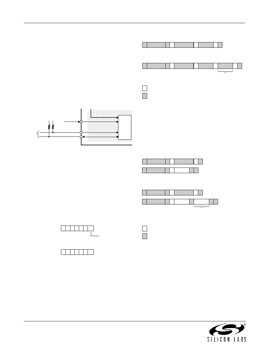
The I2C bus consists of a bidirectional serial data line
(SDA) and a serial clock input (SCL) as shown in
Figure 21. Both the SDA and SCL pins must be
connected to the VDD supply via an external pull-up as
recommended by the I2C specification.
Figure 21. I2C and Control Signals
The 7-bit device (slave) address of the Si5338 consists
of a 6-bit fixed address plus a user-selectable LSB bit as
shown in Figure 22. The LSB bit is selectable using the
optional I2C_LSB pin which is available as an ordering
option for applications that require more than one
Si5338 on a single I2C bus. Devices without the
I2C_LSB pin option have a fixed 7-bit address of 70h
addresses are also possible. See Table 17 for details on
device ordering information with the optional I2C_LSB
pin.
Figure 22. Si5338 I2C Slave Address
Data is transferred MSB first in 8-bit words as specified
by the I2C specification. A write command consists of a
7-bit device (slave) address + a write bit, an 8-bit
register address, and 8 bits of data as shown in
Figure 23. A write burst operation is also shown where
every additional data word is written using an auto-
incremented address.
Figure 23. I2C Write Operation
A read operation is performed in two stages. A data
write is used to set the register address, then a data
read is performed to retrieve the data from the set
address. A read burst operation is also supported. This
is shown in Figure 24.
Figure 24. I2C Read Operation
AC and dc electrical specifications for the SCL and SDA
pins are shown in Table 15. The timing specifications
and timing diagram for the I2C bus are compatible with
the I2C-Bus Standard. SDA timeout is supported for
compatibility with SMBus interfaces.
The I2C bus can be operated at a bus voltage of 1.71 to
3.63 V and is 3.3 V tolerant. If a bus voltage of less than
2.5 V is used, register 27[7] = 1 must be written to
maintain compatibility with the I2C bus standard.
Control
I2C_LSB
I2C_LSB/PDEC/FDEC
OEB/PINC/FINC
0/1
SCL
SDA
I
2C Bus
VDD
Slave Address
(with I2C_LSB Option)
1 1 1 0 0 0 0/1
I2C_LSB pin
0
1
2
3
4
5
6
Slave Address
(without I2C_LSB Option)
1 1 1 0 0 0
0
1
2
3
4
5
6
1 – Read
0 – Write
A – Acknowledge (SDA LOW)
N – Not Acknowledge (SDA HIGH)
S – START condition
P – STOP condition
From slave to master
From master to slave
Write Operation – Single Byte
S
0 A Reg Addr [7:0]
Slv Addr [6:0]
A Data [7:0]
P
A
Write Operation - Burst (Auto Address Increment)
Reg Addr +1
S
0 A Reg Addr [7:0]
Slv Addr [6:0]
A Data [7:0]
P
A
1 – Read
0 – Write
A – Acknowledge (SDA LOW)
N – Not Acknowledge (SDA HIGH)
S – START condition
P – STOP condition
From slave to master
From master to slave
Read Operation – Single Byte
S
0 A Reg Addr [7:0]
Slv Addr [6:0]
A P
Read Operation - Burst (Auto Address Increment)
Reg Addr +1
S
1 A
Slv Addr [6:0]
Data [7:0]
P
N
S
0 A Reg Addr [7:0]
Slv Addr [6:0]
A P
S
1 A
Slv Addr [6:0]
Data [7:0]
A
P
N
Data [7:0]
相关PDF资料 |
PDF描述 |
|---|---|
| H3AAH-2606G | IDC CABLE - HSC26H/AE26G/HSC26H |
| 0982660138 | CBL 12POS 0.5MM JMPR TYPE D 1' |
| 0982661084 | CBL 37POS 0.5MM JMPR TYPE D 6" |
| HMC08DRTH | CONN EDGECARD 16POS DIP .100 SLD |
| EBC43DCSD-S288 | CONN EDGECARD 86POS .100 EXTEND |
相关代理商/技术参数 |
参数描述 |
|---|---|
| SI5338F-A01839-GM | 制造商:Silicon Laboratories Inc 功能描述:CLOCK - Bulk |
| SI5338F-A01839-GMR | 制造商:Silicon Laboratories Inc 功能描述:CLOCK - Tape and Reel |
| Si5338F-A-GM | 功能描述:时钟发生器及支持产品 I2C-PRGRMBL clock generatr 0.16-200MHz RoHS:否 制造商:Silicon Labs 类型:Clock Generators 最大输入频率:14.318 MHz 最大输出频率:166 MHz 输出端数量:16 占空比 - 最大:55 % 工作电源电压:3.3 V 工作电源电流:1 mA 最大工作温度:+ 85 C 安装风格:SMD/SMT 封装 / 箱体:QFN-56 |
| SI5338F-A-GMR | 功能描述:时钟发生器及支持产品 I2C-Program Clk Gen 0.16-200MHz Pin-Ctrl RoHS:否 制造商:Silicon Labs 类型:Clock Generators 最大输入频率:14.318 MHz 最大输出频率:166 MHz 输出端数量:16 占空比 - 最大:55 % 工作电源电压:3.3 V 工作电源电流:1 mA 最大工作温度:+ 85 C 安装风格:SMD/SMT 封装 / 箱体:QFN-56 |
| Si5338F-B-GM | 功能描述:时钟发生器及支持产品 I2C-PRGRMBL clock generatr 0.16-200MHz RoHS:否 制造商:Silicon Labs 类型:Clock Generators 最大输入频率:14.318 MHz 最大输出频率:166 MHz 输出端数量:16 占空比 - 最大:55 % 工作电源电压:3.3 V 工作电源电流:1 mA 最大工作温度:+ 85 C 安装风格:SMD/SMT 封装 / 箱体:QFN-56 |
发布紧急采购,3分钟左右您将得到回复。