- 您现在的位置:买卖IC网 > PDF目录8951 > SI5368B-C-GQ (Silicon Laboratories Inc)IC CLK MULTIPLIER ATTEN 100TQFP PDF资料下载
参数资料
| 型号: | SI5368B-C-GQ |
| 厂商: | Silicon Laboratories Inc |
| 文件页数: | 38/92页 |
| 文件大小: | 0K |
| 描述: | IC CLK MULTIPLIER ATTEN 100TQFP |
| 标准包装: | 90 |
| 系列: | DSPLL® |
| 类型: | 时钟放大器,振动衰减器 |
| PLL: | 是 |
| 输入: | 时钟 |
| 输出: | CML,CMOS,LVDS,LVPECL |
| 电路数: | 1 |
| 比率 - 输入:输出: | 4:5 |
| 差分 - 输入:输出: | 是/是 |
| 频率 - 最大: | 808MHz |
| 除法器/乘法器: | 无/是 |
| 电源电压: | 1.71 V ~ 3.63 V |
| 工作温度: | -40°C ~ 85°C |
| 安装类型: | 表面贴装 |
| 封装/外壳: | 100-TQFP |
| 供应商设备封装: | 100-TQFP(14x14) |
| 包装: | 托盘 |
第1页第2页第3页第4页第5页第6页第7页第8页第9页第10页第11页第12页第13页第14页第15页第16页第17页第18页第19页第20页第21页第22页第23页第24页第25页第26页第27页第28页第29页第30页第31页第32页第33页第34页第35页第36页第37页当前第38页第39页第40页第41页第42页第43页第44页第45页第46页第47页第48页第49页第50页第51页第52页第53页第54页第55页第56页第57页第58页第59页第60页第61页第62页第63页第64页第65页第66页第67页第68页第69页第70页第71页第72页第73页第74页第75页第76页第77页第78页第79页第80页第81页第82页第83页第84页第85页第86页第87页第88页第89页第90页第91页第92页
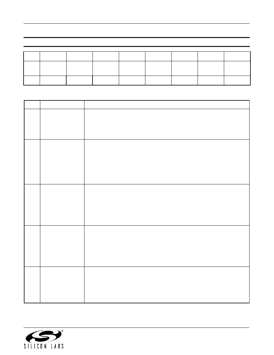
Si5368
Rev. 1.0
43
Reset value = 1111 1111
Register 21.
Bit
D7D6D5D4D3D2D1
D0
Name
INCDEC_
PIN
FSYNC_
ALIGN_PIN
CK4_ACTV
_PIN
CK3_ACTV
_PIN
CK2_ACTV
_PIN
CK1_ACTV
_PIN
CKSEL_
PIN
Type
R/W
Force 1
R/W
Bit
Name
Function
7
INCDEC_PIN
INCDEC_PIN.
Determines how coarse skew adjustments can be made. The adjustments can be
made via hardware using the INC/DEC pins or with software via the CLAT register.
0: INC and DEC inputs ignored; use CLAT register to adjust skew.
1: INC and DEC inputs control output phase increment/decrement.
6
Reserved
5
FSYNC_ALIGN_PIN FSYNC_ALIGN_PIN.
Realignment of FSYNCOUT can be controlled by the FSYNC_ALIGN input pin
instead of the FSYNC_ALIGN_REG register bit.
0: FSYNC_ALIGN pin ignored. FSYNC_ALIGN_REG register bit controls
FSYNCOUT realignment.
1: FSYNC_ALIGN pin controls FSYNCOUT realignment.
4
CK4_ACTV_PIN
CK4_ACTV_PIN.
If the CKSEL[1]/CK4_ACTV pin is functioning as the CK4_ACTV output (see
CKSEL[1]/CK4_ACTV pin description on CK4_ACTV), the CK4_ACTV_REG sta-
tus bit can be reflected to the CK4_ACTV output pin using the CK4_ACTV_PIN
enable function.
0: CK4_ACTV output pin tristated
1: CK4_ACTV status reflected to output pin.
3
CK3_ACTV_PIN
CK3_ACTV_PIN.
If the CKSEL[0]/CK3_ACTV pin is functioning as the CK3_ACTV output (see
CKSEL[0]/CK3_ACTV pin description on CK3_ACTV), the CK3_ACTV_REG sta-
tus bit can be reflected to the CK3_ACTV output pin using the CK3_ACTV_PIN
enable function.
0: CK3_ACTV output pin tristated.
1: CK3_ACTV status reflected to output pin.
2
CK2_ACTV_PIN
CK2_ACTV_PIN.
The CK2_ACTV_REG status bit can be reflected to the CK2_ACTV output pin
using the
CK2_ACTV_PIN enable function.
0: CK2_ACTV output pin tristated.
1: CK2_ACTV status reflected to output pin.
相关PDF资料 |
PDF描述 |
|---|---|
| VE-B5T-MY-F4 | CONVERTER MOD DC/DC 6.5V 50W |
| MS3456L32-7PW | CONN PLUG 35POS STRAIGHT W/PINS |
| MS3456L32-7P | CONN PLUG 35POS STRAIGHT W/PINS |
| VE-JV3-MZ-F2 | CONVERTER MOD DC/DC 24V 25W |
| VE-JV3-MZ-F1 | CONVERTER MOD DC/DC 24V 25W |
相关代理商/技术参数 |
参数描述 |
|---|---|
| SI5368B-C-GQR | 功能描述:时钟合成器/抖动清除器 Precision Clk Xplier Jitter Attn 4In/5Out RoHS:否 制造商:Skyworks Solutions, Inc. 输出端数量: 输出电平: 最大输出频率: 输入电平: 最大输入频率:6.1 GHz 电源电压-最大:3.3 V 电源电压-最小:2.7 V 封装 / 箱体:TSSOP-28 封装:Reel |
| Si5368C-B-GQ | 功能描述:锁相环 - PLL ANY-RATE CLK MULT JITTER ATTEN 5 OUTS RoHS:否 制造商:Silicon Labs 类型:PLL Clock Multiplier 电路数量:1 最大输入频率:710 MHz 最小输入频率:0.002 MHz 输出频率范围:0.002 MHz to 808 MHz 电源电压-最大:3.63 V 电源电压-最小:1.71 V 最大工作温度:+ 85 C 最小工作温度:- 40 C 封装 / 箱体:QFN-36 封装:Tray |
| SI5368C-B-GQR | 制造商:Silicon Laboratories Inc 功能描述: |
| Si5368C-C-GQ | 功能描述:锁相环 - PLL ANY-RATE CLK MULT JITTER ATTEN 5 OUTS RoHS:否 制造商:Silicon Labs 类型:PLL Clock Multiplier 电路数量:1 最大输入频率:710 MHz 最小输入频率:0.002 MHz 输出频率范围:0.002 MHz to 808 MHz 电源电压-最大:3.63 V 电源电压-最小:1.71 V 最大工作温度:+ 85 C 最小工作温度:- 40 C 封装 / 箱体:QFN-36 封装:Tray |
| SI5368C-C-GQR | 功能描述:时钟合成器/抖动清除器 Precision Clk Xplier Jitter Attn 4In/5Out RoHS:否 制造商:Skyworks Solutions, Inc. 输出端数量: 输出电平: 最大输出频率: 输入电平: 最大输入频率:6.1 GHz 电源电压-最大:3.3 V 电源电压-最小:2.7 V 封装 / 箱体:TSSOP-28 封装:Reel |
发布紧急采购,3分钟左右您将得到回复。