- 您现在的位置:买卖IC网 > PDF目录8951 > SI5368B-C-GQ (Silicon Laboratories Inc)IC CLK MULTIPLIER ATTEN 100TQFP PDF资料下载
参数资料
| 型号: | SI5368B-C-GQ |
| 厂商: | Silicon Laboratories Inc |
| 文件页数: | 45/92页 |
| 文件大小: | 0K |
| 描述: | IC CLK MULTIPLIER ATTEN 100TQFP |
| 标准包装: | 90 |
| 系列: | DSPLL® |
| 类型: | 时钟放大器,振动衰减器 |
| PLL: | 是 |
| 输入: | 时钟 |
| 输出: | CML,CMOS,LVDS,LVPECL |
| 电路数: | 1 |
| 比率 - 输入:输出: | 4:5 |
| 差分 - 输入:输出: | 是/是 |
| 频率 - 最大: | 808MHz |
| 除法器/乘法器: | 无/是 |
| 电源电压: | 1.71 V ~ 3.63 V |
| 工作温度: | -40°C ~ 85°C |
| 安装类型: | 表面贴装 |
| 封装/外壳: | 100-TQFP |
| 供应商设备封装: | 100-TQFP(14x14) |
| 包装: | 托盘 |
第1页第2页第3页第4页第5页第6页第7页第8页第9页第10页第11页第12页第13页第14页第15页第16页第17页第18页第19页第20页第21页第22页第23页第24页第25页第26页第27页第28页第29页第30页第31页第32页第33页第34页第35页第36页第37页第38页第39页第40页第41页第42页第43页第44页当前第45页第46页第47页第48页第49页第50页第51页第52页第53页第54页第55页第56页第57页第58页第59页第60页第61页第62页第63页第64页第65页第66页第67页第68页第69页第70页第71页第72页第73页第74页第75页第76页第77页第78页第79页第80页第81页第82页第83页第84页第85页第86页第87页第88页第89页第90页第91页第92页
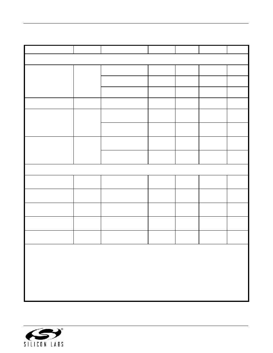
Si5368
Rev. 1.0
5
CKINn Input Pins2
Input Common Mode
Voltage (Input Thresh-
old Voltage)
VICM
1.8 V ± 5%
0.9
—
1.4
V
2.5 V ± 10%
1
—
1.7
V
3.3 V ± 10%
1.1
—
1.95
V
Input Resistance
CKNRIN
Single-ended
20
40
60
k
Single-Ended Input
Voltage Swing
(See Absolute Specs)
VISE
fCKIN < 212.5 MHz
See Figure 1.
0.2
—
VPP
fCKIN > 212.5 MHz
See Figure 1.
0.25
—
VPP
Differential Input
Voltage Swing
(See Absolute Specs)
VID
fCKIN < 212.5 MHz
See Figure 1.
0.2
—
VPP
fCKIN > 212.5 MHz
See Figure 1.
0.25
—
VPP
Output Clocks (CKOUTn)3,5,6
Common Mode
CKOVCM
LVPECL 100
load
line-to-line
VDD –1.42
—
VDD –1.25
V
Differential Output
Swing
CKOVD
LVPECL 100
load
line-to-line
1.1
—
1.9
VPP
Single Ended Output
Swing
CKOVSE
LVPECL 100
load
line-to-line
0.5
—
0.93
VPP
Differential Output Volt-
age
CKOVD
CML 100
load line-
to-line
350
425
500
mVPP
Common Mode Output
Voltage
CKOVCM
CML 100
load line-
to-line
—VDD-0.36
—
V
Table 2. DC Characteristics (Continued)
(VDD = 1.8 ± 5%, 2.5 ±10%, or 3.3 V ±10%, TA = –40 to 85 °C)
Parameter
Symbol
Test Condition
Min
Typ
Max
Unit
Notes:
1. Current draw is independent of supply voltage
2. No under- or overshoot is allowed.
3. LVPECL outputs require nominal VDD
≥ 2.5 V.
4. This is the amount of leakage that the 3-Level inputs can tolerate from an external driver. See Si53xx Family
Reference Manual for more details.
5. LVPECL, CML, LVDS and low-swing LVDS measured with Fo = 622.08 MHz.
6. The LVPECL and CMOS output formats draw more current than either LVDS or CML; however, there are restrictions in
the allowed output format pin settings so that the maximum power dissipation for the TQFP devices is limited when
they are operated at 3.3 V. When there are four enabled LVPECL or CMOS outputs, the fifth output must be disabled.
When there are five enabled outputs, there can be no more than three outputs that are either LVPECL or CMOS.
相关PDF资料 |
PDF描述 |
|---|---|
| VE-B5T-MY-F4 | CONVERTER MOD DC/DC 6.5V 50W |
| MS3456L32-7PW | CONN PLUG 35POS STRAIGHT W/PINS |
| MS3456L32-7P | CONN PLUG 35POS STRAIGHT W/PINS |
| VE-JV3-MZ-F2 | CONVERTER MOD DC/DC 24V 25W |
| VE-JV3-MZ-F1 | CONVERTER MOD DC/DC 24V 25W |
相关代理商/技术参数 |
参数描述 |
|---|---|
| SI5368B-C-GQR | 功能描述:时钟合成器/抖动清除器 Precision Clk Xplier Jitter Attn 4In/5Out RoHS:否 制造商:Skyworks Solutions, Inc. 输出端数量: 输出电平: 最大输出频率: 输入电平: 最大输入频率:6.1 GHz 电源电压-最大:3.3 V 电源电压-最小:2.7 V 封装 / 箱体:TSSOP-28 封装:Reel |
| Si5368C-B-GQ | 功能描述:锁相环 - PLL ANY-RATE CLK MULT JITTER ATTEN 5 OUTS RoHS:否 制造商:Silicon Labs 类型:PLL Clock Multiplier 电路数量:1 最大输入频率:710 MHz 最小输入频率:0.002 MHz 输出频率范围:0.002 MHz to 808 MHz 电源电压-最大:3.63 V 电源电压-最小:1.71 V 最大工作温度:+ 85 C 最小工作温度:- 40 C 封装 / 箱体:QFN-36 封装:Tray |
| SI5368C-B-GQR | 制造商:Silicon Laboratories Inc 功能描述: |
| Si5368C-C-GQ | 功能描述:锁相环 - PLL ANY-RATE CLK MULT JITTER ATTEN 5 OUTS RoHS:否 制造商:Silicon Labs 类型:PLL Clock Multiplier 电路数量:1 最大输入频率:710 MHz 最小输入频率:0.002 MHz 输出频率范围:0.002 MHz to 808 MHz 电源电压-最大:3.63 V 电源电压-最小:1.71 V 最大工作温度:+ 85 C 最小工作温度:- 40 C 封装 / 箱体:QFN-36 封装:Tray |
| SI5368C-C-GQR | 功能描述:时钟合成器/抖动清除器 Precision Clk Xplier Jitter Attn 4In/5Out RoHS:否 制造商:Skyworks Solutions, Inc. 输出端数量: 输出电平: 最大输出频率: 输入电平: 最大输入频率:6.1 GHz 电源电压-最大:3.3 V 电源电压-最小:2.7 V 封装 / 箱体:TSSOP-28 封装:Reel |
发布紧急采购,3分钟左右您将得到回复。