- 您现在的位置:买卖IC网 > PDF目录8951 > SI5368B-C-GQ (Silicon Laboratories Inc)IC CLK MULTIPLIER ATTEN 100TQFP PDF资料下载
参数资料
| 型号: | SI5368B-C-GQ |
| 厂商: | Silicon Laboratories Inc |
| 文件页数: | 81/92页 |
| 文件大小: | 0K |
| 描述: | IC CLK MULTIPLIER ATTEN 100TQFP |
| 标准包装: | 90 |
| 系列: | DSPLL® |
| 类型: | 时钟放大器,振动衰减器 |
| PLL: | 是 |
| 输入: | 时钟 |
| 输出: | CML,CMOS,LVDS,LVPECL |
| 电路数: | 1 |
| 比率 - 输入:输出: | 4:5 |
| 差分 - 输入:输出: | 是/是 |
| 频率 - 最大: | 808MHz |
| 除法器/乘法器: | 无/是 |
| 电源电压: | 1.71 V ~ 3.63 V |
| 工作温度: | -40°C ~ 85°C |
| 安装类型: | 表面贴装 |
| 封装/外壳: | 100-TQFP |
| 供应商设备封装: | 100-TQFP(14x14) |
| 包装: | 托盘 |
第1页第2页第3页第4页第5页第6页第7页第8页第9页第10页第11页第12页第13页第14页第15页第16页第17页第18页第19页第20页第21页第22页第23页第24页第25页第26页第27页第28页第29页第30页第31页第32页第33页第34页第35页第36页第37页第38页第39页第40页第41页第42页第43页第44页第45页第46页第47页第48页第49页第50页第51页第52页第53页第54页第55页第56页第57页第58页第59页第60页第61页第62页第63页第64页第65页第66页第67页第68页第69页第70页第71页第72页第73页第74页第75页第76页第77页第78页第79页第80页当前第81页第82页第83页第84页第85页第86页第87页第88页第89页第90页第91页第92页
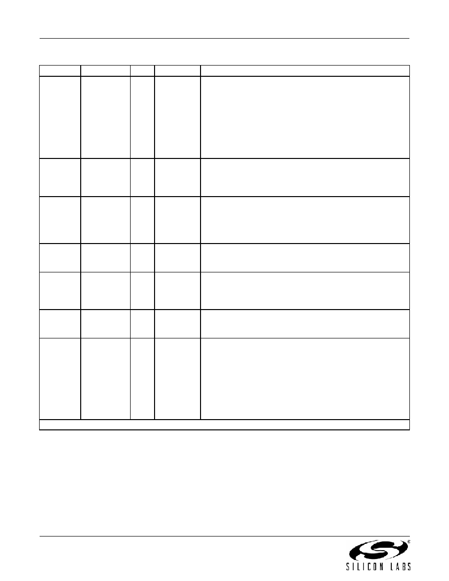
Si5368
82
Rev. 1.0
21
FS_ALIGN
I
LVCMOS
FSYNC Alignment Control.
If FSYNC_ALIGN_PIN = 1 and CK_CONFIG = 1, a logic high
on this pin causes the FS_OUT phase to be realigned to the ris-
ing edge of the currently active input sync (CKIN_3 or CKIN_4).
If FSYNC_ALIGN_PIN = 0, this pin is ignored and the
FSYNC_ALIGN_REG bit performs this function.
0 = No realignment.
1 = Realign.
This pin has a weak pull-down.
29
30
CKIN4+
CKIN4–
IMULTI
Clock Input 4.
Differential clock input. This input can also be driven with a sin-
gle-ended signal. CKIN4 serves as the frame sync input associ-
ated with the CKIN2 clock when CK_CONFIG_REG =1.
32
42
RATE0
RATE1
I
3-Level
External Crystal or Reference Clock Rate.
Three level inputs that select the type and rate of external crys-
tal or reference clock to be applied to the XA/XB port. Refer to
the Family Reference Manual for settings. These pins have both
a weak pull-up and a weak pull-down; they default to M.
34
35
CKIN2+
CKIN2–
IMULTI
Clock Input 2.
Differential input clock. This input can also be driven with a sin-
gle-ended signal.
39
40
CKIN3+
CKIN3–
IMULTI
Clock Input 3.
Differential clock input. This input can also be driven with a sin-
gle-ended signal. CKIN3 serves as the frame sync input associ-
ated with the CKIN1 clock when CK_CONFIG_REG =1.
44
45
CKIN1+
CKIN1–
IMULTI
Clock Input 1.
Differential clock input. This input can also be driven with a sin-
gle-ended signal.
49
LOL
O
LVCMOS
PLL Loss of Lock Indicator.
This pin functions as the active high PLL loss of lock indicator if
the LOL_PIN register bit is set to one.
0 = PLL locked.
1 = PLL unlocked.
If LOL_PIN = 0, this pin will tristate.
Active polarity is controlled by the LOL_POL bit. The PLL lock
status will always be reflected in the LOL_INT read only register
bit.
Table 11. Si5368 Pin Descriptions (Continued)
Pin #
Pin Name
I/O
Signal Level
Description
Note: Internal register names are indicated by underlined italics, e.g. INT_PIN. See Si5368 Register Map.
相关PDF资料 |
PDF描述 |
|---|---|
| VE-B5T-MY-F4 | CONVERTER MOD DC/DC 6.5V 50W |
| MS3456L32-7PW | CONN PLUG 35POS STRAIGHT W/PINS |
| MS3456L32-7P | CONN PLUG 35POS STRAIGHT W/PINS |
| VE-JV3-MZ-F2 | CONVERTER MOD DC/DC 24V 25W |
| VE-JV3-MZ-F1 | CONVERTER MOD DC/DC 24V 25W |
相关代理商/技术参数 |
参数描述 |
|---|---|
| SI5368B-C-GQR | 功能描述:时钟合成器/抖动清除器 Precision Clk Xplier Jitter Attn 4In/5Out RoHS:否 制造商:Skyworks Solutions, Inc. 输出端数量: 输出电平: 最大输出频率: 输入电平: 最大输入频率:6.1 GHz 电源电压-最大:3.3 V 电源电压-最小:2.7 V 封装 / 箱体:TSSOP-28 封装:Reel |
| Si5368C-B-GQ | 功能描述:锁相环 - PLL ANY-RATE CLK MULT JITTER ATTEN 5 OUTS RoHS:否 制造商:Silicon Labs 类型:PLL Clock Multiplier 电路数量:1 最大输入频率:710 MHz 最小输入频率:0.002 MHz 输出频率范围:0.002 MHz to 808 MHz 电源电压-最大:3.63 V 电源电压-最小:1.71 V 最大工作温度:+ 85 C 最小工作温度:- 40 C 封装 / 箱体:QFN-36 封装:Tray |
| SI5368C-B-GQR | 制造商:Silicon Laboratories Inc 功能描述: |
| Si5368C-C-GQ | 功能描述:锁相环 - PLL ANY-RATE CLK MULT JITTER ATTEN 5 OUTS RoHS:否 制造商:Silicon Labs 类型:PLL Clock Multiplier 电路数量:1 最大输入频率:710 MHz 最小输入频率:0.002 MHz 输出频率范围:0.002 MHz to 808 MHz 电源电压-最大:3.63 V 电源电压-最小:1.71 V 最大工作温度:+ 85 C 最小工作温度:- 40 C 封装 / 箱体:QFN-36 封装:Tray |
| SI5368C-C-GQR | 功能描述:时钟合成器/抖动清除器 Precision Clk Xplier Jitter Attn 4In/5Out RoHS:否 制造商:Skyworks Solutions, Inc. 输出端数量: 输出电平: 最大输出频率: 输入电平: 最大输入频率:6.1 GHz 电源电压-最大:3.3 V 电源电压-最小:2.7 V 封装 / 箱体:TSSOP-28 封装:Reel |
发布紧急采购,3分钟左右您将得到回复。