- 您现在的位置:买卖IC网 > PDF目录373464 > SN65LVDS302_07 (Texas Instruments, Inc.) PROGRAMMABLE 27-BIT SERIAL-TO-PARALLEL RECEIVER PDF资料下载
参数资料
| 型号: | SN65LVDS302_07 |
| 厂商: | Texas Instruments, Inc. |
| 英文描述: | PROGRAMMABLE 27-BIT SERIAL-TO-PARALLEL RECEIVER |
| 中文描述: | 可编程27位串行到并行接收机 |
| 文件页数: | 37/41页 |
| 文件大小: | 1412K |
| 代理商: | SN65LVDS302_07 |
第1页第2页第3页第4页第5页第6页第7页第8页第9页第10页第11页第12页第13页第14页第15页第16页第17页第18页第19页第20页第21页第22页第23页第24页第25页第26页第27页第28页第29页第30页第31页第32页第33页第34页第35页第36页当前第37页第38页第39页第40页第41页
www.ti.com
F/S-PIN SETTING AND CONNECTING THE SN65LVDS302 TO AN LCD DRIVER
0.0V
0.2V
0.4V
0.6V
0.8V
1.0V
1.2V
1.4V
1.6V
1.8V
2.0V
100ns
150ns
200ns
250ns
300ns
350ns
400ns
450ns
500ns
550ns
600ns
V
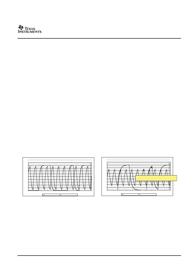
clk 22 MHz, F/S=1, CL=16 pF
data 22 Mbps, F/S=1, CL=16 pF
Application: VGA (2-channel mode); F/S set to
VDD
; Display driver load ~16 pF
(
(a)
0.0V
0.2V
0.4V
0.6V
0.8V
1.0V
1.2V
1.4V
1.6V
1.8V
2.0V
100ns
150ns
200ns
250ns
300ns
350ns
400ns
450ns
500ns
550ns
600ns
V
clk 22 MHz, F/S=0, CL=16 pF
data 22 Mbps, F/S=0, CL=16 pF
The data signal has a slower maximum switching
frequency, and therefore drives a larger amplitude
than the clock signal
Application: VGA (2-channel mode); F/S set to
GND
; Display driver load ~16 pF
(b)
SN65LVDS302
SLLS733B–JUNE 2006–REVISED FEBRUARY 2007
NOTE:
Receiver PLL tracking:
To maximize the design margin for the interconnect, good
RX PLL tracking of the TX PLL is important. FlatLink3G requires the RX PLL to have
a bandwidth higher than the bandwidth of the TX PLL. The SN65LVDS302 PLL
design is optimized to track the SN65LVDS0301 PLL particularly well, thus providing
a very large receiver skew margin. A FlatLink3G-compliant link must provide at least
±
225 ppm of receiver skew margin for the interconnect.
It is important to understand the tradeoff between power consumption, EMI, and maximum speed when selecting
the F/S signal. It is beneficial to choose the slowest rise time possible to minimize EMI and power consumption.
Unfortunately a slower rise time also reduces the timing margin left for the LCD driver. Hence it is necessary to
calculate the timing margin to select the correct F/S pin setting.
The output rise time depends on the output driver strength and the output load. An LCD driver typical capacitive
load is assumed with ~10pF. The higher the capacitive load, the slower will be the rise time. Rise time of the
SN65LVDS302 is measured as the time duration it takes the output voltage to rise from 20% of V
DD
and 80% of
V
DD
and fall time is defined as the time for the output voltage to transition from 80% of V
DD
down to 20%.
Within one mode of operation and one F/S pin setting, the rise time of the output stage is fixed and does not
adjust to the pixel frequency. Due to the short bit time at very fast pixel clock speeds and the real capacitive load
of the display driver, the output amplitude might not reach V
DD
and GND saturation fully. To ensure sufficient
signal swing and verify the design margin, it becomes necessary to determine that the output amplitude under
any circumstance reaches the display driver’s input stage logic threshold (usually 30% and 70% of V
DD
).
Figure 44
shows a worst-case rise time simulation assuming a LCD driver load of 16pF at VGA display
resolution. PCLK is the fastest switching output. With F/S set to GND (
Figure 44
-a), the PCLK output voltage
amplitude is significantly reduced. The voltage amplitude of the output data RGB[7:0], VS, HS, and DE shows
less amplitude attenuation because these outputs carry random data pattern and toggle equal or less than half
of the PCLK frequency. It is necessary to determine the timing margin between the LVDS302 output and LCD
driver input.
Figure 44. Output Amplitude as a Function of Output Toggling Frequency,
Capacitive Load and F/S Setting
37
Submit Documentation Feedback
相关PDF资料 |
PDF描述 |
|---|---|
| SN65LVDS305ZQE | PROGRAMMABLE 27-BIT DISPLAY SERIAL INTERFACE TRANSMITTER |
| SN65LVDS386EVM | Single Supply RS232C Line Driver/Receiver(?????μ?o?RS232C ?o?????????¨???2???2??????) |
| SN65LVDS387EVM | Single Supply RS232C Line Driver/Receiver(?????μ?o?RS232C ?o?????????¨???2???2??????) |
| SN65LVDT390DRG4 | HIGH-SPEED DIFFERENTIAL LINE RECEIVERS |
| SN65LVDTS33D | HIGH-SPEED DIFFERENTIAL RECEIVERS |
相关代理商/技术参数 |
参数描述 |
|---|---|
| SN65LVDS302ZQE | 功能描述:串行器/解串器 - Serdes Program 27B Display Ser Interface RoHS:否 制造商:Texas Instruments 类型:Deserializer 数据速率:1.485 Gbit/s 输入类型:ECL/LVDS 输出类型:LVCMOS 输入端数量:1 输出端数量:20 工作电源电压:2.375 V to 2.625 V 工作温度范围:0 C to + 70 C 封装 / 箱体:TQFP-64 |
| SN65LVDS302ZQER | 功能描述:串行器/解串器 - Serdes Programmable 27B Displ Ser Interface RoHS:否 制造商:Texas Instruments 类型:Deserializer 数据速率:1.485 Gbit/s 输入类型:ECL/LVDS 输出类型:LVCMOS 输入端数量:1 输出端数量:20 工作电源电压:2.375 V to 2.625 V 工作温度范围:0 C to + 70 C 封装 / 箱体:TQFP-64 |
| SN65LVDS303ZQE | 功能描述:IC PROG 27BIT SERDES TX 80-BGA RoHS:否 类别:集成电路 (IC) >> 接口 - 串行器,解串行器 系列:65LVDS 产品培训模块:Lead (SnPb) Finish for COTS Obsolescence Mitigation Program 标准包装:1 系列:- 功能:解串器 数据速率:2.5Gbps 输入类型:串行 输出类型:并联 输入数:- 输出数:24 电源电压:1.8 V ~ 3.3 V 工作温度:-40°C ~ 105°C 安装类型:表面贴装 封装/外壳:64-TQFP 裸露焊盘 供应商设备封装:64-TQFP-EP(10x10) 包装:管件 |
| SN65LVDS303ZQER | 功能描述:串行器/解串器 - Serdes QVGA-VGA 27B Display Serial Interface RoHS:否 制造商:Texas Instruments 类型:Deserializer 数据速率:1.485 Gbit/s 输入类型:ECL/LVDS 输出类型:LVCMOS 输入端数量:1 输出端数量:20 工作电源电压:2.375 V to 2.625 V 工作温度范围:0 C to + 70 C 封装 / 箱体:TQFP-64 |
| SN65LVDS304ZQER | 功能描述:串行器/解串器 - Serdes QVGAVGA 27B Display Ser Interface RoHS:否 制造商:Texas Instruments 类型:Deserializer 数据速率:1.485 Gbit/s 输入类型:ECL/LVDS 输出类型:LVCMOS 输入端数量:1 输出端数量:20 工作电源电压:2.375 V to 2.625 V 工作温度范围:0 C to + 70 C 封装 / 箱体:TQFP-64 |
发布紧急采购,3分钟左右您将得到回复。