- 您现在的位置:买卖IC网 > PDF目录98143 > ST10F252M-4T3 (STMICROELECTRONICS) 16-BIT, FLASH, 40 MHz, RISC MICROCONTROLLER, PQFP100 PDF资料下载
参数资料
| 型号: | ST10F252M-4T3 |
| 厂商: | STMICROELECTRONICS |
| 元件分类: | 微控制器/微处理器 |
| 英文描述: | 16-BIT, FLASH, 40 MHz, RISC MICROCONTROLLER, PQFP100 |
| 封装: | 14 X 14 MM, 1.40 MM HEIGHT, 0.50 MM PITCH, ROHS COMPLIANT, LQFP-100 |
| 文件页数: | 135/328页 |
| 文件大小: | 3111K |
| 代理商: | ST10F252M-4T3 |
第1页第2页第3页第4页第5页第6页第7页第8页第9页第10页第11页第12页第13页第14页第15页第16页第17页第18页第19页第20页第21页第22页第23页第24页第25页第26页第27页第28页第29页第30页第31页第32页第33页第34页第35页第36页第37页第38页第39页第40页第41页第42页第43页第44页第45页第46页第47页第48页第49页第50页第51页第52页第53页第54页第55页第56页第57页第58页第59页第60页第61页第62页第63页第64页第65页第66页第67页第68页第69页第70页第71页第72页第73页第74页第75页第76页第77页第78页第79页第80页第81页第82页第83页第84页第85页第86页第87页第88页第89页第90页第91页第92页第93页第94页第95页第96页第97页第98页第99页第100页第101页第102页第103页第104页第105页第106页第107页第108页第109页第110页第111页第112页第113页第114页第115页第116页第117页第118页第119页第120页第121页第122页第123页第124页第125页第126页第127页第128页第129页第130页第131页第132页第133页第134页当前第135页第136页第137页第138页第139页第140页第141页第142页第143页第144页第145页第146页第147页第148页第149页第150页第151页第152页第153页第154页第155页第156页第157页第158页第159页第160页第161页第162页第163页第164页第165页第166页第167页第168页第169页第170页第171页第172页第173页第174页第175页第176页第177页第178页第179页第180页第181页第182页第183页第184页第185页第186页第187页第188页第189页第190页第191页第192页第193页第194页第195页第196页第197页第198页第199页第200页第201页第202页第203页第204页第205页第206页第207页第208页第209页第210页第211页第212页第213页第214页第215页第216页第217页第218页第219页第220页第221页第222页第223页第224页第225页第226页第227页第228页第229页第230页第231页第232页第233页第234页第235页第236页第237页第238页第239页第240页第241页第242页第243页第244页第245页第246页第247页第248页第249页第250页第251页第252页第253页第254页第255页第256页第257页第258页第259页第260页第261页第262页第263页第264页第265页第266页第267页第268页第269页第270页第271页第272页第273页第274页第275页第276页第277页第278页第279页第280页第281页第282页第283页第284页第285页第286页第287页第288页第289页第290页第291页第292页第293页第294页第295页第296页第297页第298页第299页第300页第301页第302页第303页第304页第305页第306页第307页第308页第309页第310页第311页第312页第313页第314页第315页第316页第317页第318页第319页第320页第321页第322页第323页第324页第325页第326页第327页第328页
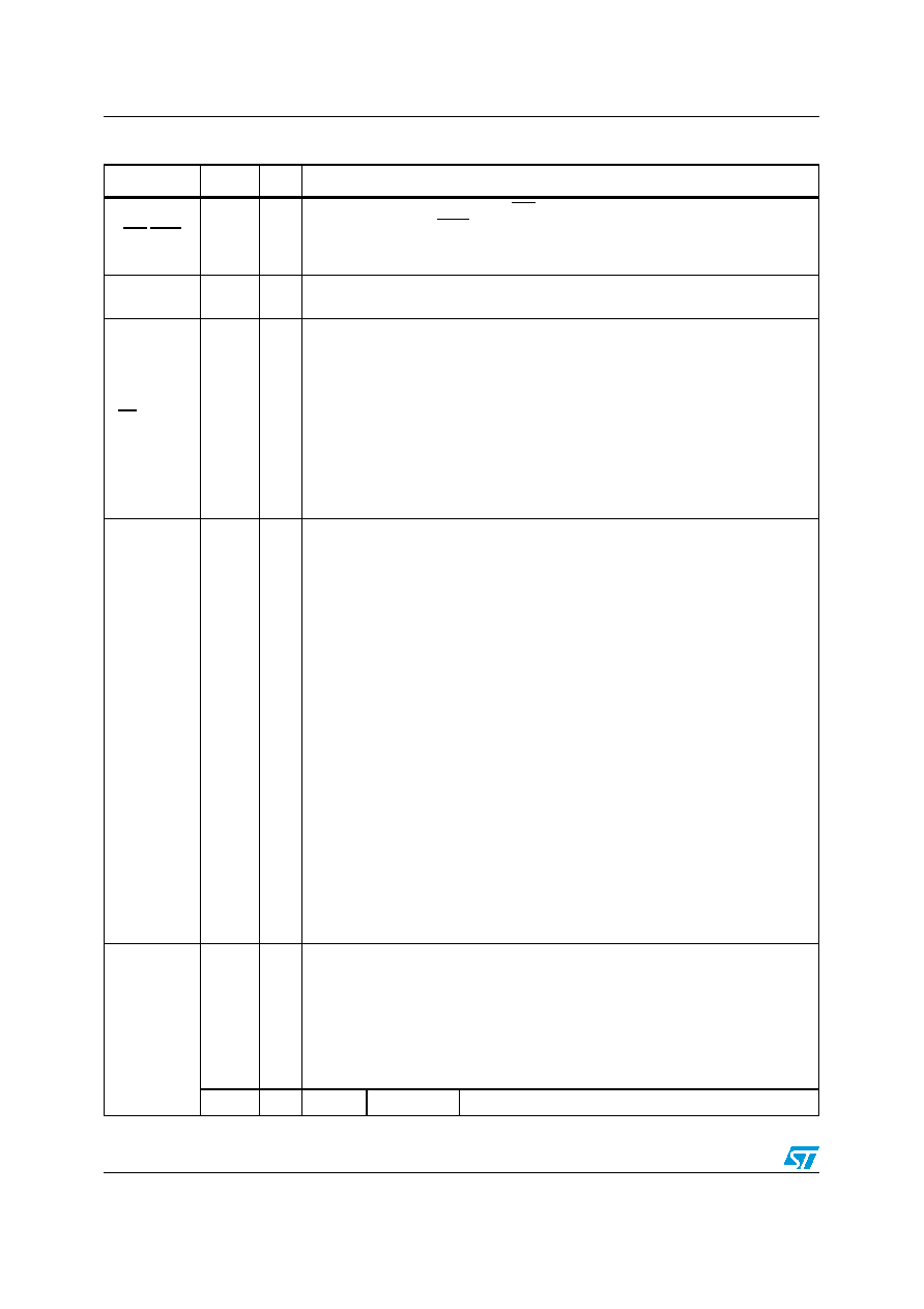
Pin data
ST10F252M
WR/WRL
57
O
External memory write strobe. In WR-mode this pin is activated for every external
data write access. In WRL-mode this pin is activated for low byte data write
accesses on a 16-bit bus, and for every data write access on an 8-bit bus. See
WRCFG in SYSCON register for mode selection.
ALE
58
O
Address latch enable output. In case of use of external addressing or of
multiplexed mode, this signal is the latch command pf the address lines.
EA / VSTBY
59
I
External access enable pin.
A low level applied to this pin during and after Reset forces the ST10F252M to start
the program from the external memory space. A high level forces ST10F252M to
start in the internal memory space. This pin is also used (when Stand-by mode is
entered, that is ST10F252M under reset and main VDD turned off) to provide a
reference voltage for the low-power embedded voltage regulator which generates
the internal 1.8V supply for the RTC module (when not disabled) and to retain data
inside the Stand-by portion of the XRAM (16 Kbyte).
It can range from 4.5 to 5.5V. In running mode, this pin can be tied low during reset
RTC and XRAM activities, since the presence of a stable VDD guarantees the
proper biasing of all those modules.
P0L.0-P0L.7,
P0H.0-P0H.7
63-70
71-78
I/O
PORT0 is a two 8-bit bidirectional I/O ports P0L and P0H, bitwise programmable
for input or output via direction bit. Programming an I/O pin as input forces the
corresponding output driver to high impedance state. The input threshold of
PORT0 is selectable (TTL or CMOS).
In case of an external bus configuration, PORT0 serves as the address (A) and as
the address / data (AD) bus in multiplexed bus modes and as the data (D) bus in
demultiplexed bus modes.
Demultiplexed bus modes
Multiplexed bus modes
The pins of P0L / P0H also serve as the additional (up to six) analog input channels
for the A/D converter, where P0L.7 equals to AN10 and P0H.x equals ANy (Analog
input channel y, where y = x + 11). This additional function has a higher priority on
demultiplexed bus function.
P1L.0-P1L.7,
P1H.0-P1H.7
79-86
89-96
I/O
PORT1 is a two 8-bit bidirectional I/O ports P1L and P1H, bitwise programmable
for input or output via direction bit. Programming an I/O pin as input forces the
corresponding output driver to high impedance state. PORT1 is used as the 16-bit
address bus (A) in demultiplexed bus modes: If at least BUSCONx is configured
such that the demultiplexed mode is selected, the pins of PORT1 are not available
for general purpose I/O function. The input threshold of PORT1 is selectable (TTL
or CMOS).
The following PORT1 pins have alternate functions:
79
O
P1L.0
XPOUT
XPWM: channel 0 output
Table 1.
Pin description (continued)
Symbol
Pin
Type
Function
Data path width
8-bit
16-bit
P0L.0 – P0L.7:
D0 – D7
D0 - D7
P0H.0 – P0H.7:
I/O
D8 - D15
Data path width
8-bit
16-bit
P0L.0 – P0L.7:
AD0 – AD7
AD0 - AD7
P0H.0 – P0H.7:
A
8 – A15
A
D8 - AD15
相关PDF资料 |
PDF描述 |
|---|---|
| ST10F269DIETR | 16-BIT, FLASH, 32 MHz, MICROCONTROLLER, UUC |
| ST10F269Z2Q3 | 16-BIT, FLASH, 40 MHz, MICROCONTROLLER, PQFP144 |
| ST10F269Z2Q6 | 16-BIT, FLASH, 40 MHz, MICROCONTROLLER, PQFP144 |
| ST10F276Z5Q3 | 16-BIT, MROM, 64 MHz, RISC MICROCONTROLLER, PQFP144 |
| ST10F296TR | 16-BIT, FLASH, 64 MHz, MICROCONTROLLER, PBGA208 |
相关代理商/技术参数 |
参数描述 |
|---|---|
| ST10F267-DT | 制造商:STMicroelectronics 功能描述: |
| ST10F267-DTR | 功能描述:16位微控制器 - MCU 16-bit MCU MAC 256 Kbyte Flash RoHS:否 制造商:Texas Instruments 核心:RISC 处理器系列:MSP430FR572x 数据总线宽度:16 bit 最大时钟频率:24 MHz 程序存储器大小:8 KB 数据 RAM 大小:1 KB 片上 ADC:Yes 工作电源电压:2 V to 3.6 V 工作温度范围:- 40 C to + 85 C 封装 / 箱体:VQFN-40 安装风格:SMD/SMT |
| ST10F268 | 制造商:STMICROELECTRONICS 制造商全称:STMicroelectronics 功能描述:16-BIT MCU WITH 256K BYTE FLASH MEMORY AND 8K BYTE RAM |
| ST10F269 | 制造商:STMICROELECTRONICS 制造商全称:STMicroelectronics 功能描述:16-BIT MCU WITH MAC UNIT, 256K BYTE FLASH MEMORY AND 12K BYTE RAM |
| ST10F269DIETR | 功能描述:MCU 16BIT 256K FLASH BARE DIE RoHS:是 类别:集成电路 (IC) >> 嵌入式 - 微控制器, 系列:ST10 标准包装:330 系列:- 核心处理器:- 芯体尺寸:8/16-位 速度:40MHz 连通性:UART/USART 外围设备:DMA,PWM,WDT 输入/输出数:32 程序存储器容量:- 程序存储器类型:外部程序存储器 EEPROM 大小:- RAM 容量:- 电压 - 电源 (Vcc/Vdd):4.5 V ~ 5.5 V 数据转换器:- 振荡器型:内部 工作温度:-40°C ~ 85°C 封装/外壳:100-BQFP 包装:管件 |
发布紧急采购,3分钟左右您将得到回复。