- 您现在的位置:买卖IC网 > PDF目录98145 > ST72E734J6D0 (STMICROELECTRONICS) 8-BIT, UVPROM, 8 MHz, MICROCONTROLLER, CDIP42 PDF资料下载
参数资料
| 型号: | ST72E734J6D0 |
| 厂商: | STMICROELECTRONICS |
| 元件分类: | 微控制器/微处理器 |
| 英文描述: | 8-BIT, UVPROM, 8 MHz, MICROCONTROLLER, CDIP42 |
| 封装: | CERAMIC, SDIP-42 |
| 文件页数: | 29/144页 |
| 文件大小: | 1280K |
| 代理商: | ST72E734J6D0 |
第1页第2页第3页第4页第5页第6页第7页第8页第9页第10页第11页第12页第13页第14页第15页第16页第17页第18页第19页第20页第21页第22页第23页第24页第25页第26页第27页第28页当前第29页第30页第31页第32页第33页第34页第35页第36页第37页第38页第39页第40页第41页第42页第43页第44页第45页第46页第47页第48页第49页第50页第51页第52页第53页第54页第55页第56页第57页第58页第59页第60页第61页第62页第63页第64页第65页第66页第67页第68页第69页第70页第71页第72页第73页第74页第75页第76页第77页第78页第79页第80页第81页第82页第83页第84页第85页第86页第87页第88页第89页第90页第91页第92页第93页第94页第95页第96页第97页第98页第99页第100页第101页第102页第103页第104页第105页第106页第107页第108页第109页第110页第111页第112页第113页第114页第115页第116页第117页第118页第119页第120页第121页第122页第123页第124页第125页第126页第127页第128页第129页第130页第131页第132页第133页第134页第135页第136页第137页第138页第139页第140页第141页第142页第143页第144页
ST72774/ST727754/ST72734
124/144
4.10.3.2 Digital A/D Conversion Result
The conversion is monotonic, meaning that the
result never decreases if the analog input does not
and never increases if the analog input does not.
If the input voltage (VAIN) is greater than or equal
to VDDA (high-level voltage reference) then the
conversion result in the DR register is FFh (full
scale) without overflow indication.
If input voltage (VAIN) is lower than or equal to
VSSA (low-level voltage reference) then the
conversion result in the DR register is 00h.
The A/D converter is linear and the digital result of
the conversion is stored in the ADCDR register.
The accuracy of the conversion is described in the
parametric section.
RAIN is the maximum recommended impedance
for an analog input signal. If the impedance is too
high, this will result in a loss of accuracy due to
leakage and sampling not being completed in the
alloted time.
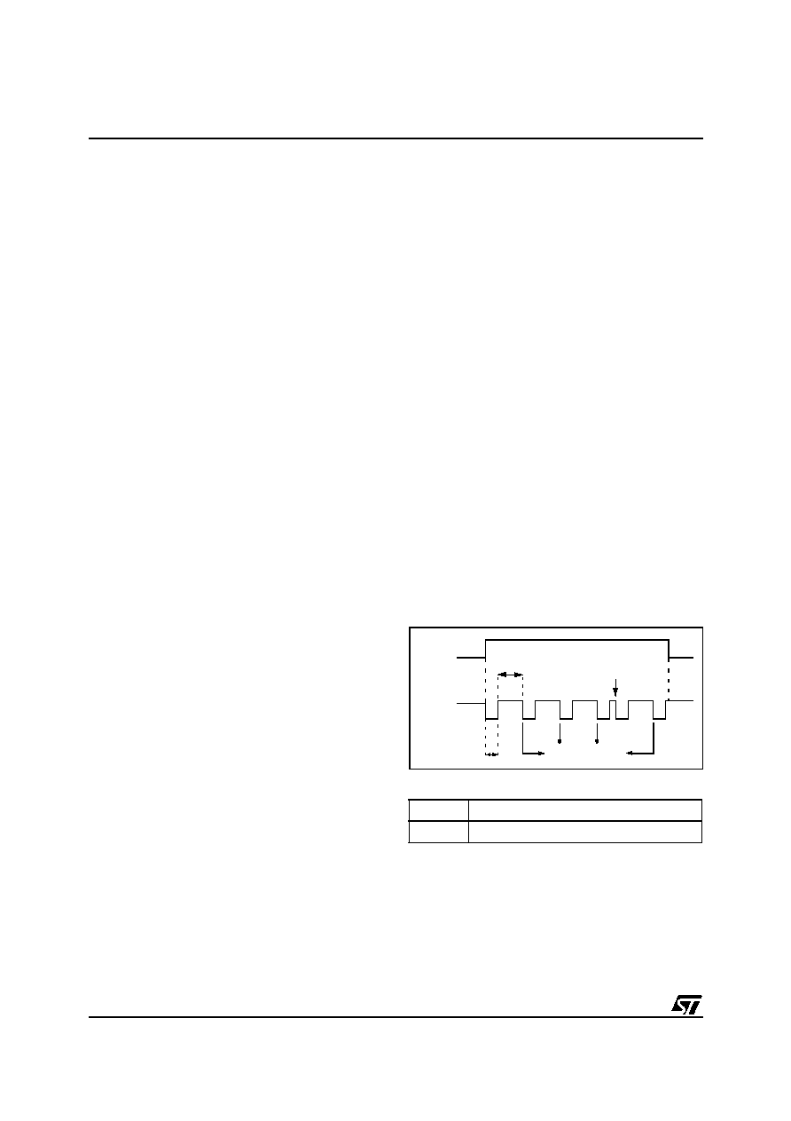
4.10.3.3 A/D Conversion Phases
The A/D conversion is based on two conversion
phases as shown in Figure 77:
s
Sample capacitor loading [duration: tLOAD]
During this phase, the VAIN input voltage to be
measured is loaded into the CADC sample
capacitor.
s
A/D conversion [duration: tCONV]
During this phase, the A/D conversion is
computed (8 successive approximations cycles)
and the CADC sample capacitor is disconnected
from the analog input pin to get the optimum
analog to digital conversion accuracy.
While the ADC is on, these two phases are
continuously repeated.
At the end of each conversion, the sample
capacitor is kept
loaded
with
the
previous
measurement
load.
The
advantage
of
this
behaviour
is
that
it
minimizes
the
current
consumption on the analog pin in case of single
input channel measurement.
4.10.3.4 Software Procedure
Refer to the control/status register (CSR) and data
register (DR) in
Section 4.10.6 for the bit
definitions and to Figure 77 for the timings.
ADC Configuration
The total duration of the A/D conversion is 12 ADC
clock periods (1/fADC=4/fCPU).
The analog input ports must be configured as
input, no pull-up, no interrupt. Refer to the I/O
ports chapter. Using these pins as analog inputs
does not affect the ability of the port to be read as
a logic input.
In the CSR register:
– Select the CH[3:0] bits to assign the analog
channel to be converted.
ADC Conversion
In the CSR register:
– Set the ADON bit to enable the A/D converter
and to start the first conversion. From this time
on, the ADC performs a continuous conver-
sion of the selected channel.
When a conversion is complete
– The COCO bit is set by hardware.
– No interrupt is generated.
– The result is in the DR register and remains
valid until the next conversion has ended.
A write to the CSR register (with ADON set) aborts
the current conversion, resets the COCO bit and
starts a new conversion.
Figure 77. ADC Conversion Timings
4.10.4 Low Power Mode
Note: The A/D converter is disabled by resetting the
ADON bit. With this feature, power consumption is
reduced when no conversion is needed and be-
tween single shot conversions.
4.10.5 Interrupts
None
Mode
Description
WAIT
No effect on A/D Converter
ADCCSR WRITE
ADON
COCO BIT SET
tLOAD
tCONV
OPERATION
HOLD
CONTROL
相关PDF资料 |
PDF描述 |
|---|---|
| ST72T774S9T1 | 8-BIT, OTPROM, 8 MHz, MICROCONTROLLER, PQFP44 |
| ST7294C6B6 | 8-BIT, MROM, 4 MHz, MICROCONTROLLER, PDIP28 |
| ST72T94C6M6 | 8-BIT, OTPROM, MICROCONTROLLER, PDSO28 |
| ST72C171K2B6 | 8-BIT, FLASH, 8 MHz, MICROCONTROLLER, PDIP32 |
| ST72E85A5G0 | 8-BIT, UVPROM, 4.332 MHz, MICROCONTROLLER, CQFP80 |
相关代理商/技术参数 |
参数描述 |
|---|---|
| ST72F260G1B5 | 功能描述:8位微控制器 -MCU Flask 4K SPI RoHS:否 制造商:Silicon Labs 核心:8051 处理器系列:C8051F39x 数据总线宽度:8 bit 最大时钟频率:50 MHz 程序存储器大小:16 KB 数据 RAM 大小:1 KB 片上 ADC:Yes 工作电源电压:1.8 V to 3.6 V 工作温度范围:- 40 C to + 105 C 封装 / 箱体:QFN-20 安装风格:SMD/SMT |
| ST72F260G1M6 | 功能描述:8位微控制器 -MCU Flash 4K SPI/I2C/SCI RoHS:否 制造商:Silicon Labs 核心:8051 处理器系列:C8051F39x 数据总线宽度:8 bit 最大时钟频率:50 MHz 程序存储器大小:16 KB 数据 RAM 大小:1 KB 片上 ADC:Yes 工作电源电压:1.8 V to 3.6 V 工作温度范围:- 40 C to + 105 C 封装 / 箱体:QFN-20 安装风格:SMD/SMT |
| ST72F260G1M6/TR | 功能描述:8位微控制器 -MCU 8B MCU FLASH OR ROM MEMORY RoHS:否 制造商:Silicon Labs 核心:8051 处理器系列:C8051F39x 数据总线宽度:8 bit 最大时钟频率:50 MHz 程序存储器大小:16 KB 数据 RAM 大小:1 KB 片上 ADC:Yes 工作电源电压:1.8 V to 3.6 V 工作温度范围:- 40 C to + 105 C 封装 / 箱体:QFN-20 安装风格:SMD/SMT |
| ST72F262G1B5 | 功能描述:8位微控制器 -MCU Flask 4K SPI RoHS:否 制造商:Silicon Labs 核心:8051 处理器系列:C8051F39x 数据总线宽度:8 bit 最大时钟频率:50 MHz 程序存储器大小:16 KB 数据 RAM 大小:1 KB 片上 ADC:Yes 工作电源电压:1.8 V to 3.6 V 工作温度范围:- 40 C to + 105 C 封装 / 箱体:QFN-20 安装风格:SMD/SMT |
| ST72F262G1B6 | 功能描述:8位微控制器 -MCU 8B MCU RoHS:否 制造商:Silicon Labs 核心:8051 处理器系列:C8051F39x 数据总线宽度:8 bit 最大时钟频率:50 MHz 程序存储器大小:16 KB 数据 RAM 大小:1 KB 片上 ADC:Yes 工作电源电压:1.8 V to 3.6 V 工作温度范围:- 40 C to + 105 C 封装 / 箱体:QFN-20 安装风格:SMD/SMT |
发布紧急采购,3分钟左右您将得到回复。