- 您现在的位置:买卖IC网 > PDF目录300038 > TMS320C6747BZKB4 (TEXAS INSTRUMENTS INC) OTHER DSP, PBGA256 PDF资料下载
参数资料
| 型号: | TMS320C6747BZKB4 |
| 厂商: | TEXAS INSTRUMENTS INC |
| 元件分类: | 数字信号处理 |
| 英文描述: | OTHER DSP, PBGA256 |
| 封装: | PLASTIC, BGA-256 |
| 文件页数: | 219/219页 |
| 文件大小: | 1557K |
| 代理商: | TMS320C6747BZKB4 |
第1页第2页第3页第4页第5页第6页第7页第8页第9页第10页第11页第12页第13页第14页第15页第16页第17页第18页第19页第20页第21页第22页第23页第24页第25页第26页第27页第28页第29页第30页第31页第32页第33页第34页第35页第36页第37页第38页第39页第40页第41页第42页第43页第44页第45页第46页第47页第48页第49页第50页第51页第52页第53页第54页第55页第56页第57页第58页第59页第60页第61页第62页第63页第64页第65页第66页第67页第68页第69页第70页第71页第72页第73页第74页第75页第76页第77页第78页第79页第80页第81页第82页第83页第84页第85页第86页第87页第88页第89页第90页第91页第92页第93页第94页第95页第96页第97页第98页第99页第100页第101页第102页第103页第104页第105页第106页第107页第108页第109页第110页第111页第112页第113页第114页第115页第116页第117页第118页第119页第120页第121页第122页第123页第124页第125页第126页第127页第128页第129页第130页第131页第132页第133页第134页第135页第136页第137页第138页第139页第140页第141页第142页第143页第144页第145页第146页第147页第148页第149页第150页第151页第152页第153页第154页第155页第156页第157页第158页第159页第160页第161页第162页第163页第164页第165页第166页第167页第168页第169页第170页第171页第172页第173页第174页第175页第176页第177页第178页第179页第180页第181页第182页第183页第184页第185页第186页第187页第188页第189页第190页第191页第192页第193页第194页第195页第196页第197页第198页第199页第200页第201页第202页第203页第204页第205页第206页第207页第208页第209页第210页第211页第212页第213页第214页第215页第216页第217页第218页当前第219页
ADV
ANCEINFORMA
TION
www.ti.com
SPRS377D – SEPTEMBER 2008 – REVISED AUGUST 2010
6.13 Memory Protection Units
The MPU performs memory protection checking. It receives requests from a bus master in the system and
checks the address against the fixed and programmable regions to see if the access is allowed. If allowed,
the transfer is passed unmodified to its output bus (to the targeted address). If the transfer is illegal (fails
the protection check) then the MPU does not pass the transfer to the output bus but rather services the
transfer internally back to the input bus (to prevent a hang) returning the fault status to the requestor as
well as generating an interrupt about the fault. The following features are supported by the MPU:
Provides memory protection for fixed and programmable address ranges
Supports multiple programmable address region
Supports secure and debug access privileges
Supports read, write, and execute access privileges
Supports privid(8) associations with ranges
Generates an interrupt when there is a protection violation, and saves violating transfer parameters
MMR access is also protected
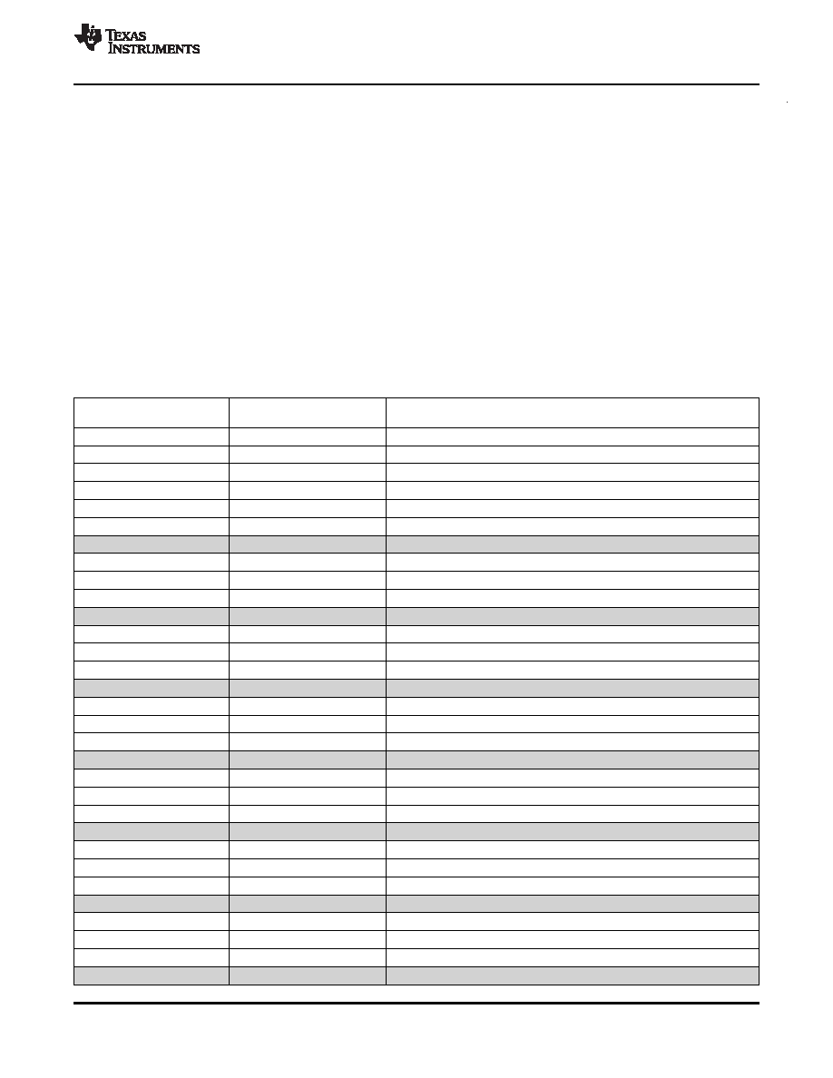
Table 6-29. MPU1 Configuration Registers
MPU1
ACRONYM
REGISTER DESCRIPTION
BYTE ADDRESS
0x01E1 4000
REVID
Revision ID
0x01E1 4004
CONFIG
Configuration
0x01E1 4010
IRAWSTAT
Interrupt raw status/set
0x01E1 4014
IENSTAT
Interrupt enable status/clear
0x01E1 4018
IENSET
Interrupt enable
0x01E1 401C
IENCLR
Interrupt enable clear
0x01E1 4020 - 0x01E1 41FF
-
Reserved
0x01E1 4200
PROG1_MPSAR
Programmable range 1, start address
0x01E1 4204
PROG1_MPEAR
Programmable range 1, end address
0x01E1 4208
PROG1_MPPA
Programmable range 1, memory page protection attributes
0x01E1 420C - 0x01E1 420F
-
Reserved
0x01E1 4210
PROG2_MPSAR
Programmable range 2, start address
0x01E1 4214
PROG2_MPEAR
Programmable range 2, end address
0x01E1 4218
PROG2_MPPA
Programmable range 2, memory page protection attributes
0x01E1 421C - 0x01E1 421F
-
Reserved
0x01E1 4220
PROG3_MPSAR
Programmable range 3, start address
0x01E1 4224
PROG3_MPEAR
Programmable range 3, end address
0x01E1 4228
PROG3_MPPA
Programmable range 3, memory page protection attributes
0x01E1 422C - 0x01E1 422F
-
Reserved
0x01E1 4230
PROG4_MPSAR
Programmable range 4, start address
0x01E1 4234
PROG4_MPEAR
Programmable range 4, end address
0x01E1 4238
PROG4_MPPA
Programmable range 4, memory page protection attributes
0x01E1 423C - 0x01E1 423F
-
Reserved
0x01E1 4240
PROG5_MPSAR
Programmable range 5, start address
0x01E1 4244
PROG5_MPEAR
Programmable range 5, end address
0x01E1 4248
PROG5_MPPA
Programmable range 5, memory page protection attributes
0x01E1 424C - 0x01E1 424F
-
Reserved
0x01E1 4250
PROG6_MPSAR
Programmable range 6, start address
0x01E1 4254
PROG6_MPEAR
Programmable range 6, end address
0x01E1 4258
PROG6_MPPA
Programmable range 6, memory page protection attributes
0x01E1 425C - 0x01E1 42FF
-
Reserved
Copyright 2008–2010, Texas Instruments Incorporated
Peripheral Information and Electrical Specifications
99
Product Folder Link(s): TMS320C6745/6747
相关PDF资料 |
PDF描述 |
|---|---|
| TMS320LF2407APGEA | 16-BIT, 20 MHz, OTHER DSP, PQFP144 |
| TMS426409AP-60DJ | 4M X 4 EDO DRAM, 60 ns, PDSO24 |
| TMS426809AP-70DGC | 2M X 8 EDO DRAM, 70 ns, PDSO28 |
| TMS44400DJ-80 | 1M X 4 FAST PAGE DRAM, 80 ns, PDSO20 |
| TMS470R1B768PGEQR | 32-BIT, FLASH, 60 MHz, RISC MICROCONTROLLER, PQFP144 |
相关代理商/技术参数 |
参数描述 |
|---|---|
| TMS320C6747BZKBA3 | 功能描述:数字信号处理器和控制器 - DSP, DSC Fixed/Floating-Point Digital Signal Proc RoHS:否 制造商:Microchip Technology 核心:dsPIC 数据总线宽度:16 bit 程序存储器大小:16 KB 数据 RAM 大小:2 KB 最大时钟频率:40 MHz 可编程输入/输出端数量:35 定时器数量:3 设备每秒兆指令数:50 MIPs 工作电源电压:3.3 V 最大工作温度:+ 85 C 封装 / 箱体:TQFP-44 安装风格:SMD/SMT |
| TMS320C6747BZKBD4 | 功能描述:数字信号处理器和控制器 - DSP, DSC Floating-Pt Dig Sig Proc RoHS:否 制造商:Microchip Technology 核心:dsPIC 数据总线宽度:16 bit 程序存储器大小:16 KB 数据 RAM 大小:2 KB 最大时钟频率:40 MHz 可编程输入/输出端数量:35 定时器数量:3 设备每秒兆指令数:50 MIPs 工作电源电压:3.3 V 最大工作温度:+ 85 C 封装 / 箱体:TQFP-44 安装风格:SMD/SMT |
| TMS320C6747BZKBT3 | 功能描述:数字信号处理器和控制器 - DSP, DSC Fixed/Floating-Point Digital Signal Proc RoHS:否 制造商:Microchip Technology 核心:dsPIC 数据总线宽度:16 bit 程序存储器大小:16 KB 数据 RAM 大小:2 KB 最大时钟频率:40 MHz 可编程输入/输出端数量:35 定时器数量:3 设备每秒兆指令数:50 MIPs 工作电源电压:3.3 V 最大工作温度:+ 85 C 封装 / 箱体:TQFP-44 安装风格:SMD/SMT |
| TMS320C6747CZKB3 | 功能描述:数字信号处理器和控制器 - DSP, DSC Fix/Floating-Pt DSP RoHS:否 制造商:Microchip Technology 核心:dsPIC 数据总线宽度:16 bit 程序存储器大小:16 KB 数据 RAM 大小:2 KB 最大时钟频率:40 MHz 可编程输入/输出端数量:35 定时器数量:3 设备每秒兆指令数:50 MIPs 工作电源电压:3.3 V 最大工作温度:+ 85 C 封装 / 箱体:TQFP-44 安装风格:SMD/SMT |
| TMS320C6747CZKB4 | 功能描述:数字信号处理器和控制器 - DSP, DSC Fix/Floating-Pt DSP RoHS:否 制造商:Microchip Technology 核心:dsPIC 数据总线宽度:16 bit 程序存储器大小:16 KB 数据 RAM 大小:2 KB 最大时钟频率:40 MHz 可编程输入/输出端数量:35 定时器数量:3 设备每秒兆指令数:50 MIPs 工作电源电压:3.3 V 最大工作温度:+ 85 C 封装 / 箱体:TQFP-44 安装风格:SMD/SMT |
发布紧急采购,3分钟左右您将得到回复。