- 您现在的位置:买卖IC网 > PDF目录300038 > TMS320C6747BZKB4 (TEXAS INSTRUMENTS INC) OTHER DSP, PBGA256 PDF资料下载
参数资料
| 型号: | TMS320C6747BZKB4 |
| 厂商: | TEXAS INSTRUMENTS INC |
| 元件分类: | 数字信号处理 |
| 英文描述: | OTHER DSP, PBGA256 |
| 封装: | PLASTIC, BGA-256 |
| 文件页数: | 42/219页 |
| 文件大小: | 1557K |
| 代理商: | TMS320C6747BZKB4 |
第1页第2页第3页第4页第5页第6页第7页第8页第9页第10页第11页第12页第13页第14页第15页第16页第17页第18页第19页第20页第21页第22页第23页第24页第25页第26页第27页第28页第29页第30页第31页第32页第33页第34页第35页第36页第37页第38页第39页第40页第41页当前第42页第43页第44页第45页第46页第47页第48页第49页第50页第51页第52页第53页第54页第55页第56页第57页第58页第59页第60页第61页第62页第63页第64页第65页第66页第67页第68页第69页第70页第71页第72页第73页第74页第75页第76页第77页第78页第79页第80页第81页第82页第83页第84页第85页第86页第87页第88页第89页第90页第91页第92页第93页第94页第95页第96页第97页第98页第99页第100页第101页第102页第103页第104页第105页第106页第107页第108页第109页第110页第111页第112页第113页第114页第115页第116页第117页第118页第119页第120页第121页第122页第123页第124页第125页第126页第127页第128页第129页第130页第131页第132页第133页第134页第135页第136页第137页第138页第139页第140页第141页第142页第143页第144页第145页第146页第147页第148页第149页第150页第151页第152页第153页第154页第155页第156页第157页第158页第159页第160页第161页第162页第163页第164页第165页第166页第167页第168页第169页第170页第171页第172页第173页第174页第175页第176页第177页第178页第179页第180页第181页第182页第183页第184页第185页第186页第187页第188页第189页第190页第191页第192页第193页第194页第195页第196页第197页第198页第199页第200页第201页第202页第203页第204页第205页第206页第207页第208页第209页第210页第211页第212页第213页第214页第215页第216页第217页第218页第219页
ADV
ANCEINFORMA
TION
SPRS377D – SEPTEMBER 2008 – REVISED AUGUST 2010
www.ti.com
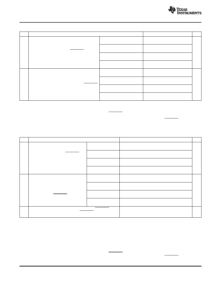
Table 6-65. Additional(1) SPI1 Master Timings, 4-Pin Chip Select Option(2) (3)
No.
PARAMATER
MIN
MAX
UNIT
Polarity = 0, Phase = 0,
2P -5
to SPI1_CLK rising
Polarity = 0, Phase = 1,
0.5tc(SPC)M + 2P -5
to SPI1_CLK rising
Delay from SPI1_SCS active to
19
td(SCS_SPC)M
ns
first SPI1_CLK(4) (5)
Polarity = 1, Phase = 0,
2P -5
to SPI1_CLK falling
Polarity = 1, Phase = 1,
0.5tc(SPC)M + 2P -5
to SPI1_CLK falling
Polarity = 0, Phase = 0,
0.5tc(SPC)M + P - 3
from SPI1_CLK falling
Polarity = 0, Phase = 1,
P - 3
Delay from final SPI1_CLK edge
from SPI1_CLK falling
20
td(SPC_SCS)M
to master deasserting SPI1_SCS
ns
Polarity = 1, Phase = 0,
(6) (7)
0.5tc(SPC)M + P -3
from SPI1_CLK rising
Polarity = 1, Phase = 1,
P - 3
from SPI1_CLK rising
(1)
These parameters are in addition to the general timings for SPI master modes (Table 6-62).
(2)
P = SYSCLK2 period
(3)
Figure shows only Polarity = 0, Phase = 0 as an example. Table gives parameters for all four master clocking modes.
(4)
In the case where the master SPI is ready with new data before SPI1_SCS assertion.
(5)
This delay can be increased under software control by the register bit field SPIDELAY.C2TDELAY[4:0].
(6)
Except for modes when SPIDAT1.CSHOLD is enabled and there is additional data to transmit. In this case, SPI1_SCS will remain
asserted.
(7)
This delay can be increased under software control by the register bit field SPIDELAY.T2CDELAY[4:0].
Table 6-66. Additional(1) SPI1 Master Timings, 5-Pin Option(2) (3)
No.
PARAMATER
MIN
MAX
UNIT
Polarity = 0, Phase = 0,
0.5tc(SPC)M+P+5
from SPI1_CLK falling
Max delay for slave to
Polarity = 0, Phase = 1,
deassert SPI1_ENA after
P+5
from SPI1_CLK falling
final SPI1_CLK edge to
18
td(SPC_ENA)M
ns
ensure master does not
Polarity = 1, Phase = 0,
0.5tc(SPC)M+P+5
begin the next
from SPI1_CLK rising
transfer.(4)
Polarity = 1, Phase = 1,
P+5
from SPI1_CLK rising
Polarity = 0, Phase = 0,
0.5tc(SPC)M + P -3
from SPI1_CLK falling
Polarity = 0, Phase = 1,
Delay from final
P - 3
from SPI1_CLK falling
SPI1_CLK edge to
20
td(SPC_SCS)M
ns
master deasserting
Polarity = 1, Phase = 0,
0.5tc(SPC)M+ P -3
SPI1_SCS (5) (6)
from SPI1_CLK rising
Polarity = 1, Phase = 1,
P - 3
from SPI1_CLK rising
Max delay for slave SPI to drive SPI1_ENA valid
21
td(SCSL_ENAL)M
after master asserts SPI1_SCS to delay the
C2TDELAY + P
ns
master from beginning the next transfer,
(1)
These parameters are in addition to the general timings for SPI master modes (Table 6-63).
(2)
P = SYSCLK2 period
(3)
Figure shows only Polarity = 0, Phase = 0 as an example. Table gives parameters for all four master clocking modes.
(4)
In the case where the master SPI is ready with new data before SPI1_ENA deassertion.
(5)
Except for modes when SPIDAT1.CSHOLD is enabled and there is additional data to transmit. In this case, SPI1_SCS will remain
asserted.
(6)
This delay can be increased under software control by the register bit field SPIDELAY.T2CDELAY[4:0].
136
Peripheral Information and Electrical Specifications
Copyright 2008–2010, Texas Instruments Incorporated
Product Folder Link(s): TMS320C6745/6747
相关PDF资料 |
PDF描述 |
|---|---|
| TMS320LF2407APGEA | 16-BIT, 20 MHz, OTHER DSP, PQFP144 |
| TMS426409AP-60DJ | 4M X 4 EDO DRAM, 60 ns, PDSO24 |
| TMS426809AP-70DGC | 2M X 8 EDO DRAM, 70 ns, PDSO28 |
| TMS44400DJ-80 | 1M X 4 FAST PAGE DRAM, 80 ns, PDSO20 |
| TMS470R1B768PGEQR | 32-BIT, FLASH, 60 MHz, RISC MICROCONTROLLER, PQFP144 |
相关代理商/技术参数 |
参数描述 |
|---|---|
| TMS320C6747BZKBA3 | 功能描述:数字信号处理器和控制器 - DSP, DSC Fixed/Floating-Point Digital Signal Proc RoHS:否 制造商:Microchip Technology 核心:dsPIC 数据总线宽度:16 bit 程序存储器大小:16 KB 数据 RAM 大小:2 KB 最大时钟频率:40 MHz 可编程输入/输出端数量:35 定时器数量:3 设备每秒兆指令数:50 MIPs 工作电源电压:3.3 V 最大工作温度:+ 85 C 封装 / 箱体:TQFP-44 安装风格:SMD/SMT |
| TMS320C6747BZKBD4 | 功能描述:数字信号处理器和控制器 - DSP, DSC Floating-Pt Dig Sig Proc RoHS:否 制造商:Microchip Technology 核心:dsPIC 数据总线宽度:16 bit 程序存储器大小:16 KB 数据 RAM 大小:2 KB 最大时钟频率:40 MHz 可编程输入/输出端数量:35 定时器数量:3 设备每秒兆指令数:50 MIPs 工作电源电压:3.3 V 最大工作温度:+ 85 C 封装 / 箱体:TQFP-44 安装风格:SMD/SMT |
| TMS320C6747BZKBT3 | 功能描述:数字信号处理器和控制器 - DSP, DSC Fixed/Floating-Point Digital Signal Proc RoHS:否 制造商:Microchip Technology 核心:dsPIC 数据总线宽度:16 bit 程序存储器大小:16 KB 数据 RAM 大小:2 KB 最大时钟频率:40 MHz 可编程输入/输出端数量:35 定时器数量:3 设备每秒兆指令数:50 MIPs 工作电源电压:3.3 V 最大工作温度:+ 85 C 封装 / 箱体:TQFP-44 安装风格:SMD/SMT |
| TMS320C6747CZKB3 | 功能描述:数字信号处理器和控制器 - DSP, DSC Fix/Floating-Pt DSP RoHS:否 制造商:Microchip Technology 核心:dsPIC 数据总线宽度:16 bit 程序存储器大小:16 KB 数据 RAM 大小:2 KB 最大时钟频率:40 MHz 可编程输入/输出端数量:35 定时器数量:3 设备每秒兆指令数:50 MIPs 工作电源电压:3.3 V 最大工作温度:+ 85 C 封装 / 箱体:TQFP-44 安装风格:SMD/SMT |
| TMS320C6747CZKB4 | 功能描述:数字信号处理器和控制器 - DSP, DSC Fix/Floating-Pt DSP RoHS:否 制造商:Microchip Technology 核心:dsPIC 数据总线宽度:16 bit 程序存储器大小:16 KB 数据 RAM 大小:2 KB 最大时钟频率:40 MHz 可编程输入/输出端数量:35 定时器数量:3 设备每秒兆指令数:50 MIPs 工作电源电压:3.3 V 最大工作温度:+ 85 C 封装 / 箱体:TQFP-44 安装风格:SMD/SMT |
发布紧急采购,3分钟左右您将得到回复。