- 您现在的位置:买卖IC网 > PDF目录98285 > TPS65040ZQER (TEXAS INSTRUMENTS INC) 8-CHANNEL POWER SUPPLY MANAGEMENT CKT, PBGA71 PDF资料下载
参数资料
| 型号: | TPS65040ZQER |
| 厂商: | TEXAS INSTRUMENTS INC |
| 元件分类: | 电源管理 |
| 英文描述: | 8-CHANNEL POWER SUPPLY MANAGEMENT CKT, PBGA71 |
| 封装: | 5 X 5 MM, 0.50 MM PITCH, GREEN, PLASTIC, MICRO, BGA-71 |
| 文件页数: | 45/73页 |
| 文件大小: | 1928K |
| 代理商: | TPS65040ZQER |
第1页第2页第3页第4页第5页第6页第7页第8页第9页第10页第11页第12页第13页第14页第15页第16页第17页第18页第19页第20页第21页第22页第23页第24页第25页第26页第27页第28页第29页第30页第31页第32页第33页第34页第35页第36页第37页第38页第39页第40页第41页第42页第43页第44页当前第45页第46页第47页第48页第49页第50页第51页第52页第53页第54页第55页第56页第57页第58页第59页第60页第61页第62页第63页第64页第65页第66页第67页第68页第69页第70页第71页第72页第73页
www.ti.com
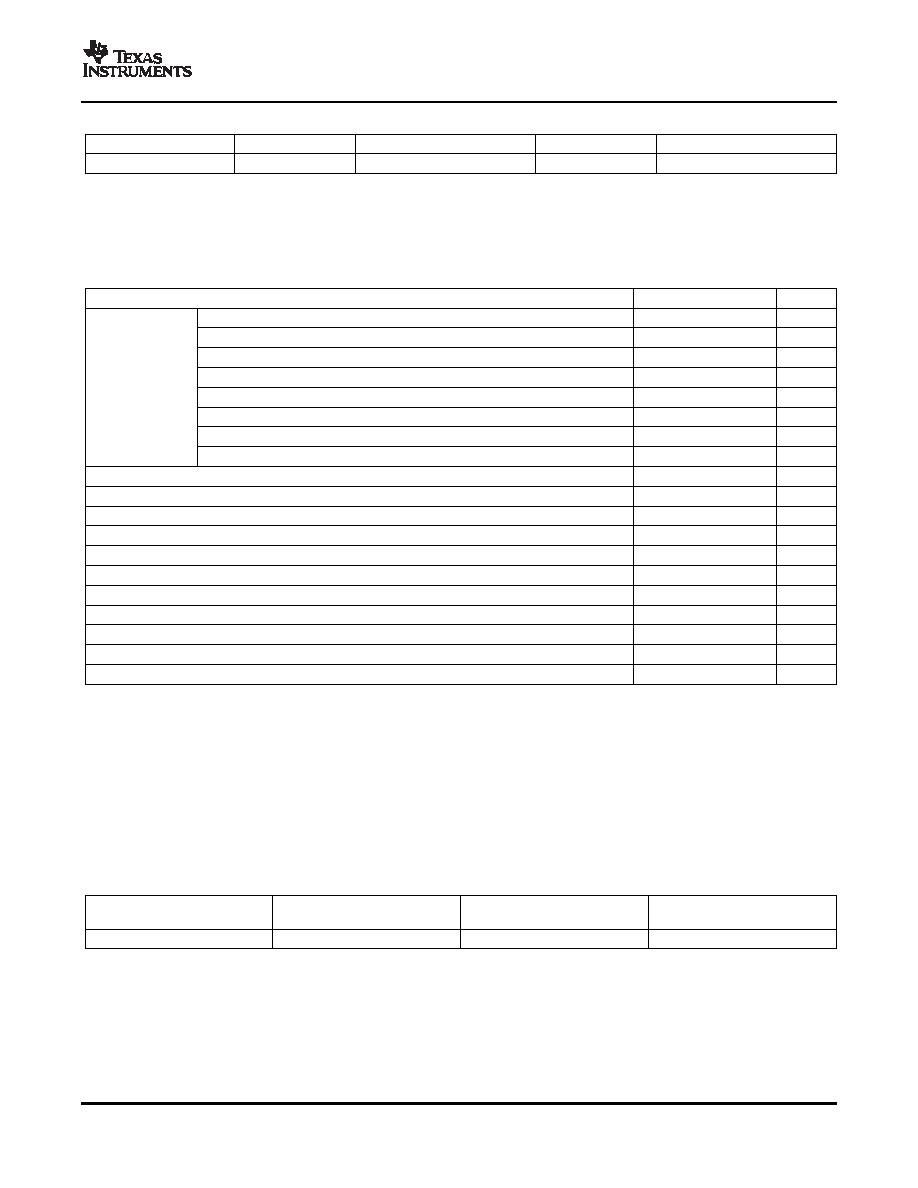
ABSOLUTE MAXIMUM RATINGS
DISSIPATION RATINGS
(1)
SLVS708B – NOVEMBER 2006 – REVISED APRIL 2007
ORDERING INFORMATION
PART NUMBER
TA
PACKAGE(1)
ORDERING
PACKAGE MARKING
TPS65040
–30
°C to 85°C
71-pin MicroStar Junior
TPS65040ZQE
PS65040
(1)
For the most current package and ordering information, see the Package Option Addendum at the end of this document, or see the TI
website at www.ti.com.
over operating free-air temperature range (unless otherwise noted) (1)
VALUE
UNIT
VIO1V8 pin with respect to GND2
–0.3 to 3.3
V
VBN1 pin with respect to GND1
–0.3 to 5.5
V
VBN2 pin with respect to GND2
–0.3 to 5.5
V
VBN3 pin with respect to GND3
–0.3 to 5.5
V
Supply voltage
VBN4 pin with respect to GND4
–0.3 to 5.5
V
VBN5 pin with respect to GND5
–0.3 to 5.5
V
VBDDP(2) pin with respect to DDGNDP(2)
–0.3 to 5.5
V
DDINA pin with respect to DDGNDA
–0.3 to 5.5
V
Input voltage range on REG_EN pin with respect to GND2
–0.3 to 5.5
V
Input voltage range on PABIAS1, PA_FB and ERR pins with respect to DDGNDA
–0.3 to 5.5
V
Input voltage range(2) on L1 and L2 pins with respect to DDGNDP
–0.3 to 5.5
V
Input voltage range on other pins(3)
–0.3 to 5.5
V
Input voltage range on SYSCLK_IN pin with respect to GND6
–0.3 to 3.3
V
Input voltage range on other input pins(4)
–0.3 to 3.3
V
Input voltage range on other pins(5)
–0.3 to 3.3
V
Peak LDO and SW output current(6)
Internally Limited
Peak current of power path(2) on VBDDP, L1, L2 pins with respect to DDGNDP
5
A
Storage temperature
–40 to 150
°C
Maximum junction temperature
125
°C
(1)
Stresses beyond those listed under absolute maximum ratings may cause permanent damage to the device. These are stress ratings
only and functional operation of the device at these or any other conditions beyond those indicated under recommended operating
conditions is not implied. Exposure to absolute-maximum-rated conditions for extended periods may affect device reliability
(2)
VBDDP is A4 and B4 pins, L1 is A5 and B5 pins, L2 is A7 and B7 pins, and DDGNDP is A6 and B6 pins.
(3)
Pin is VTCXO with respect to GND3. Pins are VGGE1_V28, VGGE2_V28, and VGGE3_V28 with respect to GND5. Pin is VOUT with
respect to DDGNDP. Pin is TEST with respect to DDGNDA.
(4)
Pins are CCLK, CDATA, CSTB, TSPCLK, TSPDIN, TSPEN, CRESET, WRFON, TXON, TXONFST, TBNDSEL1, TBNDSEL2,
SYSCLK_EN and SYSCLK_EN2 with respect to GND2.
(5)
Pins are AFC, PAVREF1, PAVREF2, and PAVREF3 with respect to GND1. Pins are SIN_SYSCLK1, SIN_SYSCLK2 and
SIN_SYSCLK3 with respect to GND6.
(6)
LDO and SW OUTPUT are V11_V28TX, PA_VDD, V12_V28RX, V_LNA_FEM, V15_V18A , V13_V28A, VTCXO, VGGE1_V28,
VGGE2_V28 and VGGE3_V28.
MAX POWER DISSIPATION
DERATING FACTOR
PACKAGE
RθJA
AT TA = 25°C
TA < 25°C
ZQE
51.23
°C/W
1.95 W
19.52 mW/
°C
(1)
Test board conditions
JEDEC High-K (2S2P) board used
3x3 inch, 4 layer
1 oz copper ground/power trace in the PCB
2 oz copper trace on the top/bottom of the PCB
5
相关PDF资料 |
PDF描述 |
|---|---|
| TPS650531IRGERQ1 | POWER SUPPLY SUPPORT CKT, PQCC24 |
| TPS650532RGET | 5-CHANNEL POWER SUPPLY SUPPORT CKT, PQCC24 |
| TPS650531RGER | 5-CHANNEL POWER SUPPLY SUPPORT CKT, PQCC24 |
| TPS65055RSMR | 1.8 A DUAL SWITCHING CONTROLLER, 2475 kHz SWITCHING FREQ-MAX, PQCC32 |
| TPS65058RGET | 1.8 A DUAL SWITCHING CONTROLLER, 2475 kHz SWITCHING FREQ-MAX, PQCC32 |
相关代理商/技术参数 |
参数描述 |
|---|---|
| TPS65050EVM-195 | 功能描述:电源管理IC开发工具 TPS65050-195 Eval Mod RoHS:否 制造商:Maxim Integrated 产品:Evaluation Kits 类型:Battery Management 工具用于评估:MAX17710GB 输入电压: 输出电压:1.8 V |
| TPS65050RSMR | 功能描述:PMIC 解决方案 6-Ch Pwr Mgmt IC RoHS:否 制造商:Texas Instruments 安装风格:SMD/SMT 封装 / 箱体:QFN-24 封装:Reel |
| TPS65050RSMRG4 | 功能描述:PMIC 解决方案 6Ch Pwr Mgmt IC RoHS:否 制造商:Texas Instruments 安装风格:SMD/SMT 封装 / 箱体:QFN-24 封装:Reel |
| TPS65050RSMT | 功能描述:PMIC 解决方案 6-Channel Power Management IC RoHS:否 制造商:Texas Instruments 安装风格:SMD/SMT 封装 / 箱体:QFN-24 封装:Reel |
| TPS65050RSMTG4 | 功能描述:PMIC 解决方案 6-Ch Pwr Mgmt IC RoHS:否 制造商:Texas Instruments 安装风格:SMD/SMT 封装 / 箱体:QFN-24 封装:Reel |
发布紧急采购,3分钟左右您将得到回复。