- 您现在的位置:买卖IC网 > PDF目录272833 > TPS65073TRSLRQ1 (TEXAS INSTRUMENTS INC) POWER SUPPLY SUPPORT CKT, PQCC48 PDF资料下载
参数资料
| 型号: | TPS65073TRSLRQ1 |
| 厂商: | TEXAS INSTRUMENTS INC |
| 元件分类: | 电源管理 |
| 英文描述: | POWER SUPPLY SUPPORT CKT, PQCC48 |
| 封装: | 6 X 6 MM, 0.4 MM PITCH, PLASTIC, QFN-48 |
| 文件页数: | 24/90页 |
| 文件大小: | 1375K |
| 代理商: | TPS65073TRSLRQ1 |
第1页第2页第3页第4页第5页第6页第7页第8页第9页第10页第11页第12页第13页第14页第15页第16页第17页第18页第19页第20页第21页第22页第23页当前第24页第25页第26页第27页第28页第29页第30页第31页第32页第33页第34页第35页第36页第37页第38页第39页第40页第41页第42页第43页第44页第45页第46页第47页第48页第49页第50页第51页第52页第53页第54页第55页第56页第57页第58页第59页第60页第61页第62页第63页第64页第65页第66页第67页第68页第69页第70页第71页第72页第73页第74页第75页第76页第77页第78页第79页第80页第81页第82页第83页第84页第85页第86页第87页第88页第89页第90页

SLVSAP7 – JANUARY 2011
www.ti.com
voltage feed-forward to achieve good line and load regulation allowing the use of small ceramic input and output
capacitors. At the beginning of each clock cycle initiated by the clock signal, the High Side MOSFET switch is
turned on. The current flows now from the input capacitor via the High Side MOSFET switch through the inductor
to the output capacitor and load. During this phase, the current ramps up until the PWM comparator trips and the
control logic will turn off the switch. The current limit comparator will also turn off the switch in case the current
limit of the High Side MOSFET switch is exceeded. After a dead time preventing shoot through current, the Low
Side MOSFET rectifier is turned on and the inductor current will ramp down. The current flows now from the
inductor to the output capacitor and to the load. It returns back to the inductor through the Low Side MOSFET
rectifier.
The next cycle will be initiated by the clock signal again turning off the Low Side MOSFET rectifier and turning on
the on the High Side MOSFET switch.
The DC-DC converters operate synchronized to each other, with converter 1 as the master. A phase shift of 180°
between converter 1 and converter 2 decreases the input RMS current. Therefore smaller input capacitors can
be used. Converter 3 operates in phase with converter 1.
DCDC1 Converter
The output voltage for converter 1 is set to a fixed voltage internally in register DEFDCDC1. The voltage can be
changed using the I2C interface. The default settings are given in Table 1.
Optionally the voltage can be set by an external resistor divider if configured in register DEFDCDC1.
DCDC2 Converter
The VDCDC2 pin must be directly connected to the DCDC2 converter's output voltage. The DCDC2 converter's
output voltage can be selected via the DEFDCDC2 pin or optionally by changing the values in registers
DEFDCDC2_LOW and DEFDCDC2_HIGH. If pin DEFDCDC2 is pulled to GND, register DEFDCDC2_LOW
defines the output voltage. If the pin DEFDCDC2 is driven HIGH, register DEFDCDC2_HIGH defines the output
voltage. Therefore, the voltage can either be changed between two values by toggling pin DEFDCDC2 or by
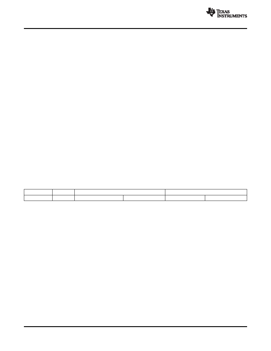
changing the register values. Default voltages for DCDC1, DCDC2 and DCDC3 are:
Table 1. Default Voltages
DCDC1
DCDC2
DCDC3
DEFDCDC2=LOW
DEFDCDC2=HIGH
DEFDCDC3=LOW
DEFDCDC3=HIGH
DCDC3 Converter
The VDCDC3 pin must be directly connected to the DCDC3 converter's output voltage. The DCDC3 converter's
output voltage can be selected via the DEFDCDC3 pin or optionally by changing the values in registers
DEFDCDC3_LOW and DEFDCDC3_HIGH. If pin DEFDCDC3 is pulled to GND, register DEFDCDC3_LOW
defines the output voltage. If the pin DEFDCDC3 is driven HIGH, register DEFDCDC3_HIGH defines the output
voltage. Therefore, the voltage can either be changed between two values by toggling pin DEFDCDC3 or by
changing the register values.
LDO2 can optionally be forced to follow the voltage defined for DCDC3 by setting Bit LDO2 TRACKING in
register DEFLDO2.
POWER SAVE MODE
The Power Save Mode is enabled by default. If the load current decreases, the converter will enter Power Save
Mode operation automatically. During Power Save Mode the converter skips switching and operates with
reduced frequency in PFM mode and with a minimum quiescent current to maintain high efficiency. The
converter will position the output voltage typically +1% above the nominal output voltage. This voltage positioning
feature minimizes voltage drops caused by a sudden load step.
The transition from PWM Mode to PFM Mode occurs once the inductor current in the Low Side MOSFET switch
becomes 0.
30
Copyright 2011, Texas Instruments Incorporated
相关PDF资料 |
PDF描述 |
|---|---|
| TC151A4924EOA713 | 0.25 A SWITCHING REGULATOR, 50 kHz SWITCHING FREQ-MAX, PDSO8 |
| TC161B3514EOA723 | 0.25 A SWITCHING REGULATOR, 100 kHz SWITCHING FREQ-MAX, PDSO8 |
| TC161B1717EOA713 | 0.25 A SWITCHING REGULATOR, 100 kHz SWITCHING FREQ-MAX, PDSO8 |
| TC161A5520EOA713 | 0.25 A SWITCHING REGULATOR, 100 kHz SWITCHING FREQ-MAX, PDSO8 |
| TC161A5825EOA713 | 0.25 A SWITCHING REGULATOR, 100 kHz SWITCHING FREQ-MAX, PDSO8 |
相关代理商/技术参数 |
参数描述 |
|---|---|
| TPS650830EVM-095 | 功能描述:TPS650830 - Power Management, Special Purpose: Mobiles Evaluation Board 制造商:texas instruments 系列:- 零件状态:有效 主要用途:电源管理,专用型: 手机 嵌入式:- 使用的 IC/零件:TPS650830 主要属性:- 辅助属性:图形用户接口,I2C 接口 所含物品:板 标准包装:1 |
| TPS650830ZAJT | 功能描述:- Converter, Mobile PCs Voltage Regulator IC 8 Output 168-NFBGA (7x7) 制造商:texas instruments 系列:- 包装:剪切带(CT) 零件状态:有效 应用:转换器,移动式个人电脑 电压 - 输入:5.4 V ~ 24 V 输出数:8 电压 - 输出:多重 工作温度:-40°C ~ 85°C 安装类型:表面贴装 封装/外壳:168-TFBGA 供应商器件封装:168-NFBGA(7x7) 标准包装:1 |
| TPS650830ZCGT | 功能描述:- Converter, Mobile PCs Voltage Regulator IC 8 Output 159-NFBGA (9x9) 制造商:texas instruments 系列:- 包装:剪切带(CT) 零件状态:有效 应用:转换器,移动式个人电脑 电压 - 输入:5.4 V ~ 24 V 输出数:8 电压 - 输出:多重 工作温度:-40°C ~ 85°C 安装类型:表面贴装 封装/外壳:159-TFBGA 供应商器件封装:159-NFBGA(9x9) 标准包装:1 |
| TPS650860A0RSKT | 功能描述:D-CAP2? Controller, Multicore, CPU, FPGA, SOC’s Voltage Regulator IC 8 Output 64-QFN (8x8) 制造商:texas instruments 系列:D-CAP2?? 包装:剪切带(CT) 零件状态:有效 应用:控制器,多核,CPU,FPGA,SOC 应用 电压 - 输入:4.5 V ~ 21 V 输出数:8 电压 - 输出:多重 工作温度:-40°C ~ 85°C 安装类型:表面贴装 封装/外壳:64-VFQFN 裸露焊盘 供应商器件封装:64-QFN(8x8) 标准包装:1 |
| TPS650860EVM-116 | 功能描述:EVALUATION MODULE 制造商:texas instruments 系列:* 零件状态:在售 标准包装:1 |
发布紧急采购,3分钟左右您将得到回复。