- 您现在的位置:买卖IC网 > PDF目录272833 > TPS65073TRSLRQ1 (TEXAS INSTRUMENTS INC) POWER SUPPLY SUPPORT CKT, PQCC48 PDF资料下载
参数资料
| 型号: | TPS65073TRSLRQ1 |
| 厂商: | TEXAS INSTRUMENTS INC |
| 元件分类: | 电源管理 |
| 英文描述: | POWER SUPPLY SUPPORT CKT, PQCC48 |
| 封装: | 6 X 6 MM, 0.4 MM PITCH, PLASTIC, QFN-48 |
| 文件页数: | 27/90页 |
| 文件大小: | 1375K |
| 代理商: | TPS65073TRSLRQ1 |
第1页第2页第3页第4页第5页第6页第7页第8页第9页第10页第11页第12页第13页第14页第15页第16页第17页第18页第19页第20页第21页第22页第23页第24页第25页第26页当前第27页第28页第29页第30页第31页第32页第33页第34页第35页第36页第37页第38页第39页第40页第41页第42页第43页第44页第45页第46页第47页第48页第49页第50页第51页第52页第53页第54页第55页第56页第57页第58页第59页第60页第61页第62页第63页第64页第65页第66页第67页第68页第69页第70页第71页第72页第73页第74页第75页第76页第77页第78页第79页第80页第81页第82页第83页第84页第85页第86页第87页第88页第89页第90页
/RESET
THRESHOLD
Vbat
delay
Vref=1V
+
-
RESET
Vbat
THRESHOLD
T RESET
comparator
output(internal)
www.ti.com
SLVSAP7 – JANUARY 2011
Optionally, there is internal sequencing for the DCDC converters and both LDOs available. Bits DCDC_SQ[0..2]
in register CON_CTRL1 define the start-up and shut-down sequence for the DCDC converters. Depending on
the sequencing option, the signal at EN_DCDC1, EN_DCDC2 and EN_DCDC3 are ignored. For automatic
internal sequencing, the enable signals which are not used should be connected to GND.
LDO1 and LDO2 will start up automatically as defined in register LDO_CTRL1. See details about the sequencing
options in the register description for CON_CTRL1 and LDO_CTRL1.
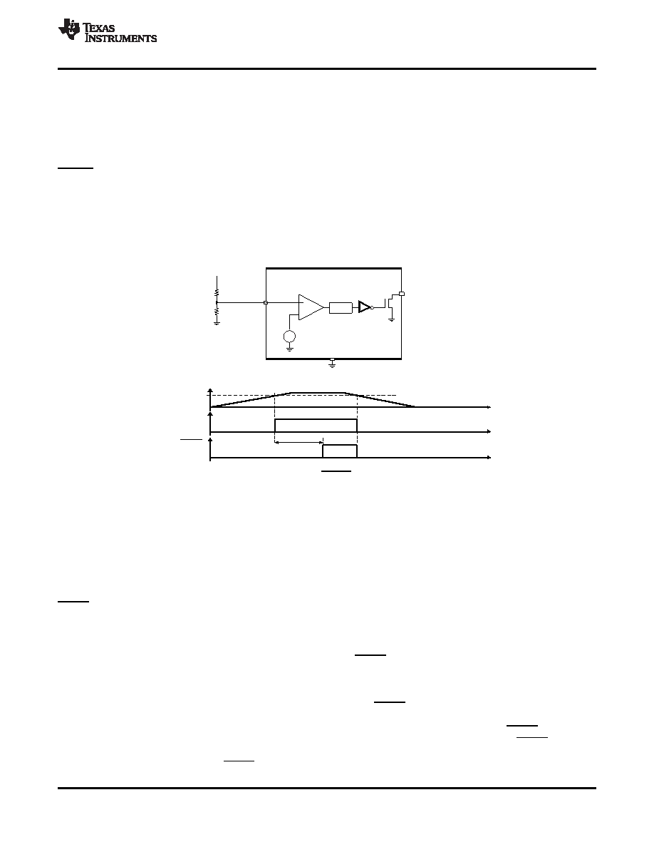
RESET
The contain circuitry that can generate a reset pulse for a processor with a certain delay time. The input voltage
at a comparator is sensed at an input called THRESHOLD. When the voltage exceeds the threshold, the output
goes high with the delay time defined in register PGOOD. The reset circuitry is not active in OFF-state. The
pull-up resistor for this open drain output must not be connected directly to the battery as this may cause a
leakage path when the power path (SYS voltage) is turned off. The reset delay time equals the setting for the
PGOOD signal.
Figure 32. Reset Timing
PGOOD (reset signal for applications processor)
This open drain output generates a power-good signal depending on the status of the power good Bits for the
DCDC converters and the LDOs. Register PGOODMASK defines which of the power good Bits of the converters
and LDOs are used to drive the external PGOOD signal low when the voltage is below the target value. If e.g.,
Bit MASK DCDC2 is set to 1, the PGOOD pin will be driven low as long as the output of DCDC2 is below the
target voltage. If the output voltage of DCDC2 rises to its nominal value, the PGOOD pin will be released after
the delay time defined. See the default settings in the register description.
PB_IN (Push-button IN)
This pin is the ON/OFF button for the PMU to leave OFF-state and enter ON-state by pulling this pin to GND.
Entering ON-state will first ramp the output voltage of the power path (SYS), load the default register settings and
start up the DCDC converters and LDOs with the sequencing defined. In ON-state, the I2C interface is active and
the wLED converter can be enabled. The system turns on if PB_IN is pulled LOW for >50ms (debounce time)
AND the output voltage of the power path manager is above the undervoltage lockout voltage (AVDD6 > 3V).
This is for Vbat>3V OR VAC>3V OR VUSB>3V. The default voltage for the undervoltage lockout voltage can be
changed with Bits <UVLO1>, <UVLO0> in register CON_CTRL2. The value will be valid until the device was
turned off completely by entering Off state. The system turns off if PB_IN is released OR the system voltage falls
below the undervoltage lockout voltage of 3V. This is the case when either the battery voltage drops below 3.0V
or the input voltage at the pins AC or USB is below 3V. In order to keep the enabled after PB_IN is released
HIGH, there is an input pin called POWER_ON which needs to be pulled HIGH before the PB_IN button is
released. POWER_ON=HIGH will typically be asserted by the application processor to keep the PMU in
ON-state after the power button at PB_IN is released.
Copyright 2011, Texas Instruments Incorporated
33
相关PDF资料 |
PDF描述 |
|---|---|
| TC151A4924EOA713 | 0.25 A SWITCHING REGULATOR, 50 kHz SWITCHING FREQ-MAX, PDSO8 |
| TC161B3514EOA723 | 0.25 A SWITCHING REGULATOR, 100 kHz SWITCHING FREQ-MAX, PDSO8 |
| TC161B1717EOA713 | 0.25 A SWITCHING REGULATOR, 100 kHz SWITCHING FREQ-MAX, PDSO8 |
| TC161A5520EOA713 | 0.25 A SWITCHING REGULATOR, 100 kHz SWITCHING FREQ-MAX, PDSO8 |
| TC161A5825EOA713 | 0.25 A SWITCHING REGULATOR, 100 kHz SWITCHING FREQ-MAX, PDSO8 |
相关代理商/技术参数 |
参数描述 |
|---|---|
| TPS650830EVM-095 | 功能描述:TPS650830 - Power Management, Special Purpose: Mobiles Evaluation Board 制造商:texas instruments 系列:- 零件状态:有效 主要用途:电源管理,专用型: 手机 嵌入式:- 使用的 IC/零件:TPS650830 主要属性:- 辅助属性:图形用户接口,I2C 接口 所含物品:板 标准包装:1 |
| TPS650830ZAJT | 功能描述:- Converter, Mobile PCs Voltage Regulator IC 8 Output 168-NFBGA (7x7) 制造商:texas instruments 系列:- 包装:剪切带(CT) 零件状态:有效 应用:转换器,移动式个人电脑 电压 - 输入:5.4 V ~ 24 V 输出数:8 电压 - 输出:多重 工作温度:-40°C ~ 85°C 安装类型:表面贴装 封装/外壳:168-TFBGA 供应商器件封装:168-NFBGA(7x7) 标准包装:1 |
| TPS650830ZCGT | 功能描述:- Converter, Mobile PCs Voltage Regulator IC 8 Output 159-NFBGA (9x9) 制造商:texas instruments 系列:- 包装:剪切带(CT) 零件状态:有效 应用:转换器,移动式个人电脑 电压 - 输入:5.4 V ~ 24 V 输出数:8 电压 - 输出:多重 工作温度:-40°C ~ 85°C 安装类型:表面贴装 封装/外壳:159-TFBGA 供应商器件封装:159-NFBGA(9x9) 标准包装:1 |
| TPS650860A0RSKT | 功能描述:D-CAP2? Controller, Multicore, CPU, FPGA, SOC’s Voltage Regulator IC 8 Output 64-QFN (8x8) 制造商:texas instruments 系列:D-CAP2?? 包装:剪切带(CT) 零件状态:有效 应用:控制器,多核,CPU,FPGA,SOC 应用 电压 - 输入:4.5 V ~ 21 V 输出数:8 电压 - 输出:多重 工作温度:-40°C ~ 85°C 安装类型:表面贴装 封装/外壳:64-VFQFN 裸露焊盘 供应商器件封装:64-QFN(8x8) 标准包装:1 |
| TPS650860EVM-116 | 功能描述:EVALUATION MODULE 制造商:texas instruments 系列:* 零件状态:在售 标准包装:1 |
发布紧急采购,3分钟左右您将得到回复。