- 您现在的位置:买卖IC网 > PDF目录20614 > USB-EA-CONVZ (Analog Devices Inc)SUPPORT BOARD ADUC8XX PDF资料下载
参数资料
| 型号: | USB-EA-CONVZ |
| 厂商: | Analog Devices Inc |
| 文件页数: | 16/68页 |
| 文件大小: | 0K |
| 描述: | SUPPORT BOARD ADUC8XX |
| 标准包装: | 1 |
| 类型: | 仿真器 |
| 适用于相关产品: | ADuC8xx |
| 所含物品: | 模块 |
第1页第2页第3页第4页第5页第6页第7页第8页第9页第10页第11页第12页第13页第14页第15页当前第16页第17页第18页第19页第20页第21页第22页第23页第24页第25页第26页第27页第28页第29页第30页第31页第32页第33页第34页第35页第36页第37页第38页第39页第40页第41页第42页第43页第44页第45页第46页第47页第48页第49页第50页第51页第52页第53页第54页第55页第56页第57页第58页第59页第60页第61页第62页第63页第64页第65页第66页第67页第68页
REV. B
ADuC824
–23–
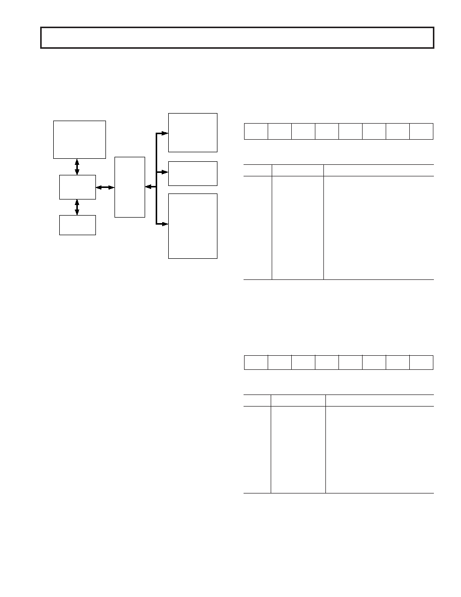
The SFR space is mapped to the upper 128 bytes of internal data
memory space and accessed by direct addressing only. It provides
an interface between the CPU and all on-chip peripherals. A block
diagram showing the programming model of the ADuC824 via
the SFR area is shown in Figure 16. A complete SFR map is shown
in Figure 17.
128-BYTE
SPECIAL
FUNCTION
REGISTER
AREA
8 KBYTE
ELECTRICALLY
REPROGRAMMABLE
NONVOLATILE
FLASH/EE PROGRAM
MEMORY
8051-
COMPATIBLE
CORE
OTHER ON-CHIP
PERIPHERALS
TEMPERATURE
SENSOR
CURRENT
SOURCES
12-BIT DAC
SERIAL I/O
WDT
PSM
TIC
PLL
DUAL
SIGMA-DELTA ADCs
640-BYTE
ELECTRICALLY
REPROGRAMMABLE
NONVOLATILE
FLASH/EE DATA
MEMORY
256 BYTES
RAM
Figure 16. Programming Model
OVERVIEW OF MCU-RELATED SFRs
Accumulator SFR
ACC is the Accumulator register and is used for math operations
including addition, subtraction, integer multiplication and division,
and Boolean bit manipulations. The mnemonics for accumulator-
specific instructions refer to the Accumulator as A.
B SFR
The B register is used with the ACC for multiplication and divi-
sion operations. For other instructions it can be treated as a
general-purpose scratchpad register.
Stack Pointer SFR
The SP register is the stack pointer and is used to hold an internal
RAM address that is called the ‘top of the stack.’ The SP register is
incremented before data is stored during PUSH and CALL execu-
tions. While the stack may reside anywhere in on-chip RAM, the
SP register is initialized to 07H after a reset. This causes the
stack to begin at location 08H.
Data Pointer
The Data Pointer is made up of three 8-bit registers, named
DPP (page byte), DPH (high byte), and DPL (low byte).
These are used to provide memory addresses for internal and
external code access and external data access. It may be ma-
nipulated as a 16-bit register (DPTR = DPH, DPL), although
INC DPTR instructions will automatically carry over to DPP, or
as three independent 8-bit registers (DPP, DPH, DPL).
Program Status Word SFR
The PSW register is the Program Status Word which contains
several bits reflecting the current status of the CPU as detailed in
Table I.
SFR Address
D0H
Power ON Default Value
00H
Bit Addressable
Yes
Y
CC
A0
F1
S
R0
S
RV
O1
FP
Table I. PSW SFR Bit Designations
Bit
Name
Description
7
CY
Carry Flag
6
AC
Auxiliary Carry Flag
5
F0
General-Purpose Flag
4
RS1
Register Bank Select Bits
3
RS0
RS1
RS0
Selected Bank
000
011
102
113
2
OV
Overflow Flag
1
F1
General-Purpose Flag
0
P
Parity Bit
Power Control SFR
The Power Control (PCON) register contains bits for power-
saving options and general-purpose status flags as shown in
Table II.
SFR Address
87H
Power ON Default Value
00H
Bit Addressable
No
D
O
M
SD
P
I
R
E
SD
P
0
T
N
IF
F
O
E
L
A1
F
G0
F
GD
PL
D
I
Table II. PCON SFR Bit Designations
Bit
Name
Description
7
SMOD
Double UART Baud Rate
6
SERIPD
I
2C/SPI Power-Down Interrupt
Enable
5
INT0PD
INT0 Power-Down Interrupt
Enable
4
ALEOFF
Disable ALE Output
3
GF1
General-Purpose Flag Bit
2
GF0
General-Purpose Flag Bit
1
PD
Power-Down Mode Enable
0
IDL
Idle Mode Enable
相关PDF资料 |
PDF描述 |
|---|---|
| RGP10KE-E3/54 | DIODE GPP 1A 800V 500NS DO-41 |
| A7NXB-1506G | CABLE D-SUB - AMN15B/AE15G/X |
| C1005C0G1H470J | CAP CER 47PF 50V 5% NP0 0402 |
| SLF6045T-220M1R1-3PF | INDUCTOR POWER 22UH 1.1A SMD |
| GBM12DRTI-S13 | CONN EDGECARD 24POS .156 EXTEND |
相关代理商/技术参数 |
参数描述 |
|---|---|
| USB-ETH ADAPTER | 制造商:DANAHER - FLUKE 功能描述:USB TO 10/100MBPS ETHERNET ADAPTER |
| USB-ETHERNET-AX88772B | 制造商:Olimex 功能描述:USB ETH ADAPTOR OLINUXINO |
| USB-EVAL | 功能描述:界面开发工具 USB products evalua- tion board unpopultd RoHS:否 制造商:Bourns 产品:Evaluation Boards 类型:RS-485 工具用于评估:ADM3485E 接口类型:RS-485 工作电源电压:3.3 V |
| USBEX02 | 制造商:Distributed By MCM 功能描述:15' USB 2.0 Active Extension Cable |
| USBEXT-150 | 制造商:DigitHead Inc 功能描述:USB EXTENDER 150' |
发布紧急采购,3分钟左右您将得到回复。