- 您现在的位置:买卖IC网 > PDF目录20614 > USB-EA-CONVZ (Analog Devices Inc)SUPPORT BOARD ADUC8XX PDF资料下载
参数资料
| 型号: | USB-EA-CONVZ |
| 厂商: | Analog Devices Inc |
| 文件页数: | 31/68页 |
| 文件大小: | 0K |
| 描述: | SUPPORT BOARD ADUC8XX |
| 标准包装: | 1 |
| 类型: | 仿真器 |
| 适用于相关产品: | ADuC8xx |
| 所含物品: | 模块 |
第1页第2页第3页第4页第5页第6页第7页第8页第9页第10页第11页第12页第13页第14页第15页第16页第17页第18页第19页第20页第21页第22页第23页第24页第25页第26页第27页第28页第29页第30页当前第31页第32页第33页第34页第35页第36页第37页第38页第39页第40页第41页第42页第43页第44页第45页第46页第47页第48页第49页第50页第51页第52页第53页第54页第55页第56页第57页第58页第59页第60页第61页第62页第63页第64页第65页第66页第67页第68页
REV. B
ADuC824
–37–
Calibration
The ADuC824 provides four calibration modes that can be pro-
grammed via the mode bits in the ADCMODE SFR detailed in
Table IV. In fact, every ADuC824 has already been factory
calibrated. The resultant Offset and Gain calibration coefficients
for both the primary and auxiliary ADCs are stored on-chip
in manufacturing-specific Flash/EE memory locations. At power-
on, these factory calibration coefficients are automatically
downloaded to the calibration registers in the ADuC824 SFR
space. Each ADC (primary and auxiliary) has dedicated calibration
SFRs, these have been described earlier as part of the general
ADC SFR description. However, the factory calibration values
in the ADC calibration SFRs will be overwritten if any one of
the four calibration options are initiated and that ADC is enabled
via the ADC enable bits in ADCMODE.
Even though an internal offset calibration mode is described
below, it should be recognized that both ADCs are chopped. This
chopping scheme inherently minimizes offset and means that an
internal offset calibration should never be required. Also, because
factory 5 V/25
°C gain calibration coefficients are automatically
present at power-on, an internal full-scale calibration will only
be required if the part is being operated at 3 V or at temperatures
significantly different from 25
°C.
The ADuC824 offers “internal” or “system” calibration facilities.
For full calibration to occur on the selected ADC, the calibration
logic must record the modulator output for two different input
conditions. These are zero-scale and full-scale points. These
points are derived by performing a conversion on the different
input voltages provided to the input of the modulator during
calibration. The result of the zero-scale calibration conversion is
stored in the Offset Calibration Registers for the appropriate
ADC. The result of the “full-scale” calibration conversion is
stored in the Gain Calibration Registers for the appropriate
ADC. With these readings, the calibration logic can calculate
the offset and the gain slope for the input-to-output transfer
function of the converter.
During an “internal” zero-scale or full-scale calibration, the re-
spective “zero” input and full-scale input are automatically
connected to the ADC input pins internally to the device. A
“system” calibration, however, expects the system zero-scale and
system full-scale voltages to be applied to the external ADC pins
before the calibration mode is initiated. In this way external ADC
errors are taken into account and minimized as a result of system
calibration. It should also be noted that to optimize calibration
accuracy, all ADuC824 ADC calibrations are carried out auto-
matically at the slowest update rate.
Internally in the ADuC824, the coefficients are normalized before
being used to scale the words coming out of the digital filter. The
offset calibration coefficient is subtracted from the result prior to
the multiplication by the gain coefficient. All ADuC824 ADC
specifications will only apply after a zero-scale and full-scale
calibration at the operating point (supply voltage/temperature)
of interest.
From an operational point of view, a calibration should be treated
like another ADC conversion. A zero-scale calibration (if required)
should always be carried out before a full-scale calibration. System
software should monitor the relevant ADC RDY0/1 bit in the
ADCSTAT SFR to determine end of calibration via a polling
sequence or interrupt driven routine.
NONVOLATILE FLASH/EE MEMORY
Flash/EE Memory Overview
The ADuC824 incorporates Flash/EE memory technology on-chip
to provide the user with nonvolatile, in-circuit reprogrammable,
code and data memory space.
Flash/EE memory is a relatively recent type of nonvolatile memory
technology and is based on a single transistor cell architecture.
This technology is basically an outgrowth of EPROM technology
and was developed through the late 1980s. Flash/EE memory takes
the flexible in-circuit reprogrammable features of EEPROM and
combines them with the space efficient/density features of EPROM
(see Figure 26).
Because Flash/EE technology is based on a single transistor cell
architecture, a Flash memory array, like EPROM, can be imple-
mented to achieve the space efficiencies or memory densities
required by a given design.
Like EEPROM, Flash memory can be programmed in-system at
a byte level, although it must first be erased; the erase being per-
formed in page blocks. Thus, Flash memory is often and more
correctly referred to as Flash/EE memory.
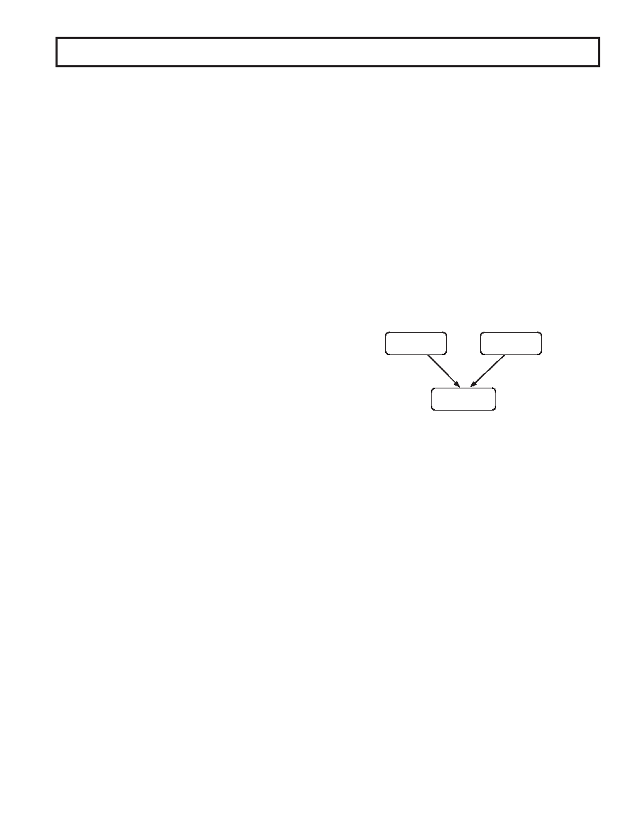
FLASH/EE MEMORY
TECHNOLOGY
SPACE EFFICIENT/
DENSITY
IN-CIRCUIT
REPROGRAMMABLE
EPROM
TECHNOLOGY
EEPROM
TECHNOLOGY
Figure 26. Flash/EE Memory Development
Overall, Flash/EE memory represents a step closer to the ideal
memory device that includes nonvolatility, in-circuit programma-
bility, high density, and low cost. Incorporated in the ADuC824,
Flash/EE memory technology allows the user to update program
code space in-circuit, without the need to replace one-time
programmable (OTP) devices at remote operating nodes.
Flash/EE Memory and the ADuC824
The ADuC824 provides two arrays of Flash/EE Memory for user
applications. 8 Kbytes of Flash/EE Program space are provided
on-chip to facilitate code execution without any external discrete
ROM device requirements. The program memory can be pro-
grammed using conventional third party memory programmers.
This array can also be programmed in-circuit, using the serial
download mode provided.
A 640-Byte Flash/EE Data Memory space is also provided on-chip.
This may be used as a general-purpose nonvolatile scratchpad
area. User access to this area is via a group of six SFRs. This space
can be programmed at a byte level, although it must first be
erased in 4-byte pages.
ADuC824 Flash/EE Memory Reliability
The Flash/EE Program and Data Memory arrays on the ADuC824
are fully qualified for two key Flash/EE memory characteristics,
namely Flash/EE Memory Cycling Endurance and Flash/EE
Memory Data Retention.
相关PDF资料 |
PDF描述 |
|---|---|
| RGP10KE-E3/54 | DIODE GPP 1A 800V 500NS DO-41 |
| A7NXB-1506G | CABLE D-SUB - AMN15B/AE15G/X |
| C1005C0G1H470J | CAP CER 47PF 50V 5% NP0 0402 |
| SLF6045T-220M1R1-3PF | INDUCTOR POWER 22UH 1.1A SMD |
| GBM12DRTI-S13 | CONN EDGECARD 24POS .156 EXTEND |
相关代理商/技术参数 |
参数描述 |
|---|---|
| USB-ETH ADAPTER | 制造商:DANAHER - FLUKE 功能描述:USB TO 10/100MBPS ETHERNET ADAPTER |
| USB-ETHERNET-AX88772B | 制造商:Olimex 功能描述:USB ETH ADAPTOR OLINUXINO |
| USB-EVAL | 功能描述:界面开发工具 USB products evalua- tion board unpopultd RoHS:否 制造商:Bourns 产品:Evaluation Boards 类型:RS-485 工具用于评估:ADM3485E 接口类型:RS-485 工作电源电压:3.3 V |
| USBEX02 | 制造商:Distributed By MCM 功能描述:15' USB 2.0 Active Extension Cable |
| USBEXT-150 | 制造商:DigitHead Inc 功能描述:USB EXTENDER 150' |
发布紧急采购,3分钟左右您将得到回复。