- 您现在的位置:买卖IC网 > PDF目录20614 > USB-EA-CONVZ (Analog Devices Inc)SUPPORT BOARD ADUC8XX PDF资料下载
参数资料
| 型号: | USB-EA-CONVZ |
| 厂商: | Analog Devices Inc |
| 文件页数: | 32/68页 |
| 文件大小: | 0K |
| 描述: | SUPPORT BOARD ADUC8XX |
| 标准包装: | 1 |
| 类型: | 仿真器 |
| 适用于相关产品: | ADuC8xx |
| 所含物品: | 模块 |
第1页第2页第3页第4页第5页第6页第7页第8页第9页第10页第11页第12页第13页第14页第15页第16页第17页第18页第19页第20页第21页第22页第23页第24页第25页第26页第27页第28页第29页第30页第31页当前第32页第33页第34页第35页第36页第37页第38页第39页第40页第41页第42页第43页第44页第45页第46页第47页第48页第49页第50页第51页第52页第53页第54页第55页第56页第57页第58页第59页第60页第61页第62页第63页第64页第65页第66页第67页第68页
REV. B
ADuC824
–38–
Endurance quantifies the ability of the Flash/EE memory to be
cycled through many Program, Read, and Erase cycles. In real
terms, a single endurance cycle is composed of four independent,
sequential events. These events are defined as:
a. initial page erase sequence
b. read/verify sequence
A single Flash/EE
c. byte program sequence
Memory
d. second read/verify sequence
Endurance Cycle
In reliability qualification, every byte in both the program and
data Flash/EE memory is cycled from 00 hex to FFhex until a
first fail is recorded signifying the endurance limit of the on-chip
Flash/EE memory.
As indicated in the specification pages of this data sheet, the
ADuC824 Flash/EE Memory Endurance qualification has been
carried out in accordance with JEDEC Specification A117 over
the industrial temperature range of –40
°C, +25°C, and +85°C.
The results allow the specification of a minimum endurance figure
over supply and temperature of 100,000 cycles, with an endurance
figure of 700,000 cycles being typical of operation at 25
°C.
Retention quantifies the ability of the Flash/EE memory to retain
its programmed data over time. Again, the ADuC824 has been
qualified in accordance with the formal JEDEC Retention Life-
time Specification (A117) at a specific junction temperature
(TJ = 55
°C). As part of this qualification procedure, the Flash/EE
memory is cycled to its specified endurance limit described above,
before data retention is characterized. This means that the Flash/
EE memory is guaranteed to retain its data for its full specified
retention lifetime every time the Flash/EE memory is repro-
grammed. It should also be noted that retention lifetime, based
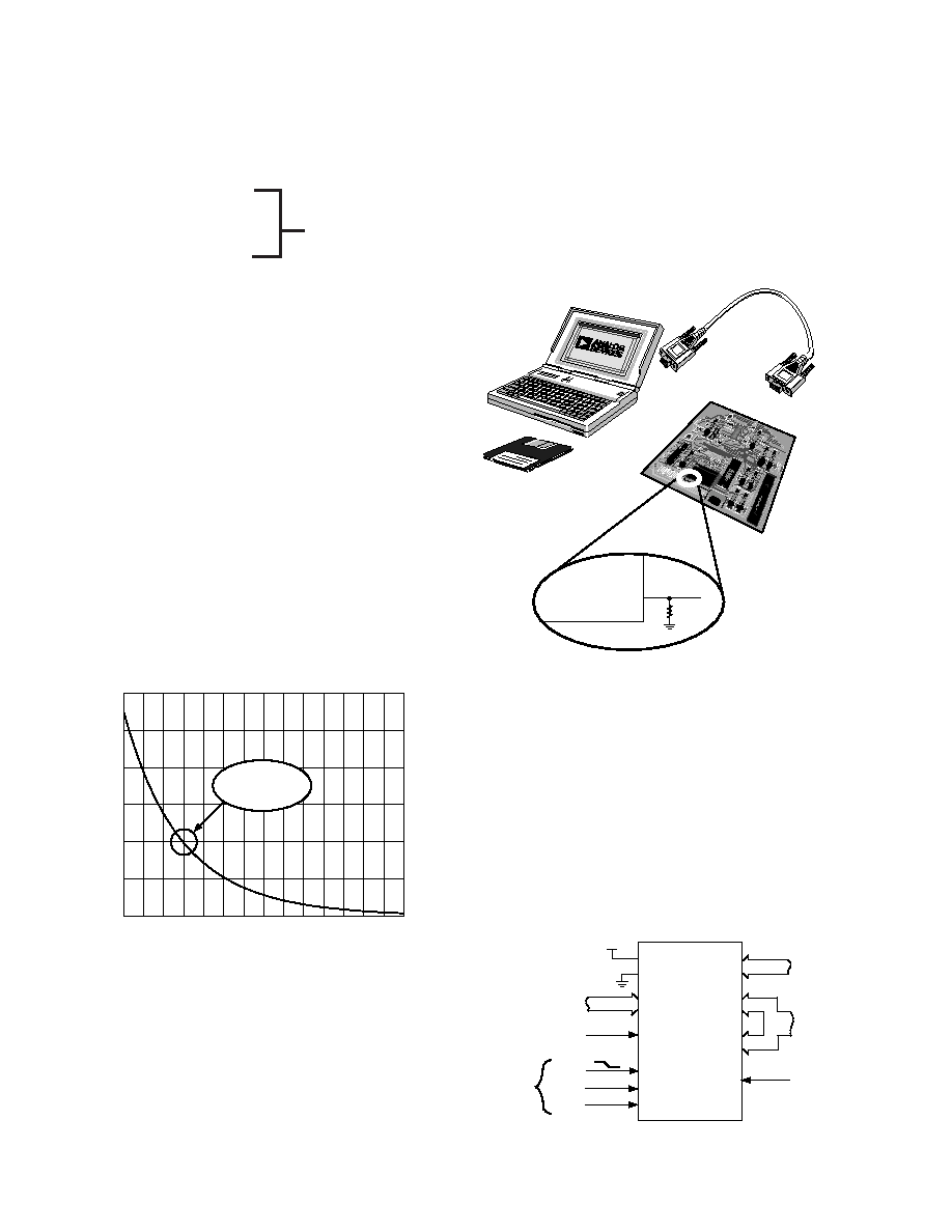
on an activation energy of 0.6 eV, will derate with TJ as shown
in Figure 27.
40
60
70
90
TJ JUNCTION TEMPERATURE – C
RETENTION
–
Years
250
200
150
100
50
0
50
80
110
300
100
ADI SPECIFICATION
100 YEARS MIN.
AT T
J = 55 C
Figure 27. Flash/EE Memory Data Retention
Using the Flash/EE Program Memory
The 8 Kbyte Flash/EE Program Memory array is mapped
into the lower 8 Kbytes of the 64 Kbytes program space
addressable by the ADuC824, and is used to hold user code
in typical applications.
The program memory Flash/EE memory arrays can be pro-
grammed in one of two modes, namely:
Serial Downloading (In-Circuit Programming)
As part of its factory boot code, the ADuC824 facilitates serial
code download via the standard UART serial port. Serial down-
load mode is automatically entered on power-up if the external
pin,
PSEN, is pulled low through an external resistor as shown
in Figure 28. Once in this mode, the user can download code to
the program memory array while the device is sited in its target
application hardware. A PC serial download executable is pro-
vided as part of the ADuC824 QuickStart development system.
The Serial Download protocol is detailed in a MicroConverter
Applications Note uC004 available from the ADI MicroConverter
Website at www.analog.com/microconverter.
PSEN
ADuC824
PULL
PSEN LOW DURING RESET
TO CONFIGURE THE ADuC824
FOR SERIAL DOWNLOAD MODE
1k
Figure 28. Flash/EE Memory Serial Download Mode
Programming
Parallel Programming
The parallel programming mode is fully compatible with conven-
tional third party Flash or EEPROM device programmers. A
block diagram of the external pin configuration required to support
parallel programming is shown in Figure 29. In this mode, Ports 0,
1, and 2 operate as the external data and address bus interface,
ALE operates as the Write Enable strobe, and Port 3 is used as a
general configuration port that configures the device for various
program and erase operations during parallel programming.
The high voltage (12 V) supply required for Flash/EE program-
ming is generated using on-chip charge pumps to supply the high
voltage program lines.
VDD
GND
P3
PSEN
RESET
P0
P1
P2
ALE
ADuC824
5V
PROGRAM MODE
(SEE TABLE XII)
GND
PROGRAM
DATA
(D0–D7)
PROGRAM
ADDRESS
(A0–A13)
(P2.0 = A0)
(P1.7 = A13)
WRITE ENABLE
STROBE
COMMAND
ENABLE
P3.0
NEGATIVE
EDGE
P3.6
ENTRY
SEQUENCE
VDD
Figure 29. Flash/EE Memory Parallel Programming
相关PDF资料 |
PDF描述 |
|---|---|
| RGP10KE-E3/54 | DIODE GPP 1A 800V 500NS DO-41 |
| A7NXB-1506G | CABLE D-SUB - AMN15B/AE15G/X |
| C1005C0G1H470J | CAP CER 47PF 50V 5% NP0 0402 |
| SLF6045T-220M1R1-3PF | INDUCTOR POWER 22UH 1.1A SMD |
| GBM12DRTI-S13 | CONN EDGECARD 24POS .156 EXTEND |
相关代理商/技术参数 |
参数描述 |
|---|---|
| USB-ETH ADAPTER | 制造商:DANAHER - FLUKE 功能描述:USB TO 10/100MBPS ETHERNET ADAPTER |
| USB-ETHERNET-AX88772B | 制造商:Olimex 功能描述:USB ETH ADAPTOR OLINUXINO |
| USB-EVAL | 功能描述:界面开发工具 USB products evalua- tion board unpopultd RoHS:否 制造商:Bourns 产品:Evaluation Boards 类型:RS-485 工具用于评估:ADM3485E 接口类型:RS-485 工作电源电压:3.3 V |
| USBEX02 | 制造商:Distributed By MCM 功能描述:15' USB 2.0 Active Extension Cable |
| USBEXT-150 | 制造商:DigitHead Inc 功能描述:USB EXTENDER 150' |
发布紧急采购,3分钟左右您将得到回复。