- 您现在的位置:买卖IC网 > PDF目录225499 > V58C2128404SBLT6I (PROMOS TECHNOLOGIES INC) 32M X 4 DDR DRAM, 0.7 ns, PDSO66 PDF资料下载
参数资料
| 型号: | V58C2128404SBLT6I |
| 厂商: | PROMOS TECHNOLOGIES INC |
| 元件分类: | DRAM |
| 英文描述: | 32M X 4 DDR DRAM, 0.7 ns, PDSO66 |
| 封装: | 0.400 X 0.875 INCH, PLASTIC, MS-024FC, TSOP2-66 |
| 文件页数: | 35/60页 |
| 文件大小: | 915K |
| 代理商: | V58C2128404SBLT6I |
第1页第2页第3页第4页第5页第6页第7页第8页第9页第10页第11页第12页第13页第14页第15页第16页第17页第18页第19页第20页第21页第22页第23页第24页第25页第26页第27页第28页第29页第30页第31页第32页第33页第34页当前第35页第36页第37页第38页第39页第40页第41页第42页第43页第44页第45页第46页第47页第48页第49页第50页第51页第52页第53页第54页第55页第56页第57页第58页第59页第60页
40
V58C2128(804/404/164)SB*I Rev. 1.3 March 2006
ProMOS TECHNOLOGIES
V58C2128(804/404/164)SB*I
NOTES: (continued)
23. The refresh period 64ms. This equates to an average refresh rate of 7.8s.
24. The I/O capacitance per DQS and DQ byte/group will not differ by more than this maximum amount for any
given device.
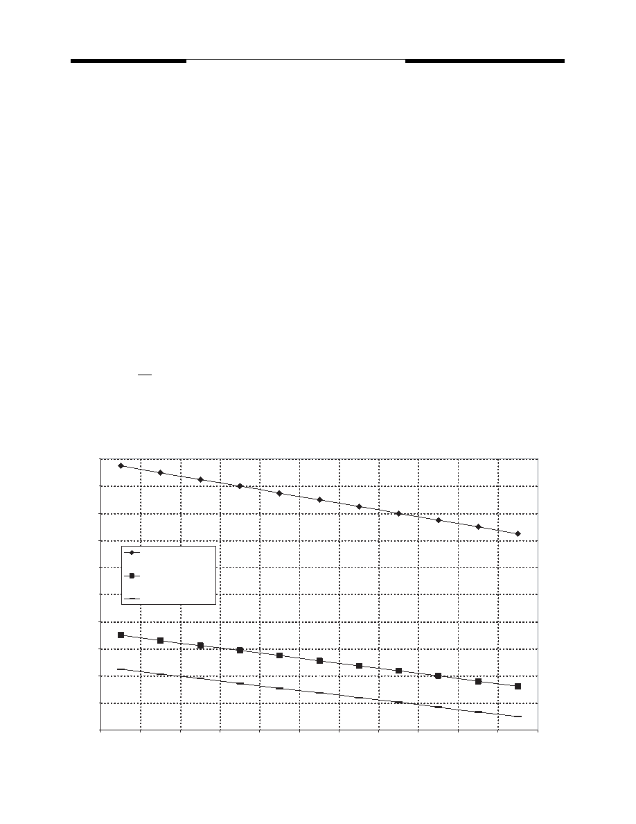
25. The valid data window is derived by achieving other specifications - tHP (tCK/2), tDQSQ, and tQH
(tQH = tHP - tQHS). The data valid window derates directly proportional with the clock duty cycle and a practical data
valid window can be derived. The clock is allowed a maximum duty cycle variation of 45/55. Functionality is uncertain
when operating beyond a 45/55 ratio. The data valid window derating curves are provided below for duty cycles rang-
ing between 50/50 and 45/55.
26. Referenced to each output group: x4 = DQS with DQ0-DQ3; x8 = DQS with DQ0-DQ7; x16 = LDQS with DQ0-
DQ7; and UDQS with DQ8-DQ15.
27. This limit is actually a nominal value and does not result in a fail value. CKE is HIGH during REFRESH command
period (tRFC [MIN]) else CKE is LOW (i.e., during standby).
28. To maintain a valid level, the transitioning edge of the input must:
a) Sustain a constant slew rate from the current AC level through to the target AC level, VIL(AC) or VIH(AC).
b) Reach at least the target AC level.
c) After the AC target level is reached, continue to maintain at least the target DC level, VIL(DC) or VIH(DC).
29. The Input capacitance per pin group will not differ by more than this maximum amount for any given device..
30. CK and CK input slew rate must be 1V/ns.
31. DQ and DM input slew rates must not deviate from DQS by more than 10%. If the DQ/DM/DQS slew rate is less
than 0.5V/ns, timing must be derated: 50ps must be added to tDS and tDH for each 100mv/ns reduction in slew rate.
If slew rate exceeds 4V/ns, functionality is uncertain.
32. VDD must not vary more than 4% if CKE is not active while any bank is active.
3.8
3.750
3.700
3.650
3.600
3.550
3.500
3.450
3.400
3.350
3.300
3.250
50/50
49.5/50.5
49/51
48.5/52.5
48/52
47.5/53.5
47/53
46.5/54.5
46/54
45.5/55.5
45/55
2.463
2.500
2.425
2.388
2.350
2.313
2.275
2.238
2.200
2.163
2.125
3.6
3.4
3.2
3.0
2.8
2.6
2.4
2.2
2.0
1.8
-7 @tCK = 10ns
-7 @tCK = 7.5ns
-7 @tCK = 7ns
ns
相关PDF资料 |
PDF描述 |
|---|---|
| V58C365164S5 | 4M X 16 DDR DRAM, 0.1 ns, PDSO66 |
| V608ME06 | VCO, 1900 MHz - 2270 MHz |
| V603ME07 | VCO, 1896 MHz - 1924 MHz |
| V6049001 | VCO, 1600 MHz - 2200 MHz |
| V610ME04 | VCO, 1950 MHz - 2150 MHz |
相关代理商/技术参数 |
参数描述 |
|---|---|
| V58C2128804S | 制造商:MOSEL 制造商全称:MOSEL 功能描述:HIGH PERFORMANCE 2.5 VOLT 128 Mbit DDR SDRAM |
| V58C2256 | 制造商:MOSEL 制造商全称:MOSEL 功能描述:HIGH PERFORMANCE 2.5 VOLT 256 Mbit DDR SDRAM |
| V58C2256164S | 制造商:MOSEL 制造商全称:MOSEL 功能描述:HIGH PERFORMANCE 2.5 VOLT 256 Mbit DDR SDRAM |
| V58C2256324SAB30 | 制造商:Marvell 功能描述:Marvell V58C2256324SAB30 |
| V58C2256324SAB33 | 制造商:Marvell 功能描述:Marvell V58C2256324SAB33 |
发布紧急采购,3分钟左右您将得到回复。