- 您现在的位置:买卖IC网 > PDF目录68560 > W987X6CBN80 (WINBOND ELECTRONICS CORP) 8M X 16 SYNCHRONOUS DRAM, 6 ns, PBGA54 PDF资料下载
参数资料
| 型号: | W987X6CBN80 |
| 厂商: | WINBOND ELECTRONICS CORP |
| 元件分类: | DRAM |
| 英文描述: | 8M X 16 SYNCHRONOUS DRAM, 6 ns, PBGA54 |
| 封装: | 8 X 9 MM, 1.20 MM HEIGHT, FBGA-54 |
| 文件页数: | 42/46页 |
| 文件大小: | 1634K |
| 代理商: | W987X6CBN80 |
第1页第2页第3页第4页第5页第6页第7页第8页第9页第10页第11页第12页第13页第14页第15页第16页第17页第18页第19页第20页第21页第22页第23页第24页第25页第26页第27页第28页第29页第30页第31页第32页第33页第34页第35页第36页第37页第38页第39页第40页第41页当前第42页第43页第44页第45页第46页
Preliminary W987X6CB
Publication Release Date: June 6, 2002
- 5 -
Revision A1
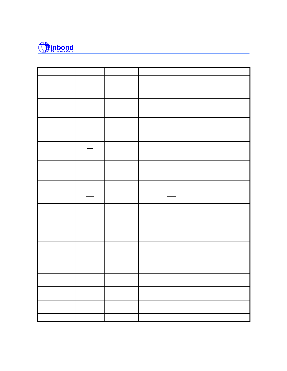
5. BALL DESCRIPTION
PIN NUMBER
BALL NAME
FUNCTION
DESCRIPTION
H7, H8, J8, J7,
J3, J2, H3, H2,
H1, G3, H9, G2
A0
A11
Address
Multiplexed pins for row and column address.
Row address: A0
A11. Column address: A0 A8.
G7, G8
BS0, BS1
Bank Select
Select bank to activate during row address latch
time, or bank to read/write during address latch
time.
A8, B9, B8, C9,
C8, D9, D8, E9,
E1, D2 D1, C2,
C1, B2, B1, A2
DQ0
DQ15
Data Input/
Output
Multiplexed pins for data output and input.
G9
CS
Chip Select
Disable or enable the command decoder. When
command decoder is disabled, new command is
ignored and previous operation continues.
F8
RAS
Row Address
Strobe
Command input. When sampled at the rising edge
of the clock, RAS , CAS and WE define the
operation to be executed.
F7
CAS
Column
Address Strobe
Referred to RAS
F9
WE
Write Enable
Referred to RAS
F1, E8
UDQM
LDQM
Input/Output
Mask
The output buffer is placed at Hi-Z (with latency of
2) when DQM is sampled high in read cycle. In write
cycle, sampling DQM high will block the write
operation with zero latency.
F2
CLK
Clock Inputs
System clock used to sample inputs on the rising
edge of clock.
F3
CKE
Clock Enable
CKE controls the clock activation and deactivation.
When CKE is low, Power Down mode, Suspend
mode or Self Refresh mode is entered.
A9, E7, J9
VDD
Power
Power for input buffers and logic circuit inside
DRAM.
A1, E3, J1
VSS
Ground
Ground for input buffers and logic circuit inside
DRAM.
A7, B3, C7, D3
VDDQ
Power for I/O
Buffer
Separated power from VCC, used for output buffers
to improve noise.
A3, B7, C3, D7
VSSQ
Ground for I/O
Buffer
Separated ground from VSS, used for output buffers
to improve noise.
E2, G1
NC
No Connection No connection
相关PDF资料 |
PDF描述 |
|---|---|
| W987X6CBG75 | 8M X 16 SYNCHRONOUS DRAM, 5.4 ns, PBGA54 |
| W987Y6CBG80 | 8M X 16 SYNCHRONOUS DRAM, 6 ns, PBGA54 |
| W987Z6CHG75 | 8M X 16 SYNCHRONOUS DRAM, 5.4 ns, PDSO54 |
| W989D2CBJX6E | 16M X 32 DDR DRAM, 5.4 ns, PBGA90 |
| W989D6CBGX7E | 32M X 16 DDR DRAM, 5.4 ns, PBGA54 |
相关代理商/技术参数 |
参数描述 |
|---|---|
| W987Y6CBN | 制造商:未知厂家 制造商全称:未知厂家 功能描述:DRAM |
| W987Z6CBN | 制造商:未知厂家 制造商全称:未知厂家 功能描述:DRAM |
| W988D2FB | 制造商:WINBOND 制造商全称:Winbond 功能描述:256Mb Mobile LPSDR |
| W988D2FBJX6E | 制造商:Winbond Electronics Corp 功能描述:IC LPSDR SDRAM 256MBIT 90VFBGA |
| W988D2FBJX6I | 制造商:WINBOND 制造商全称:Winbond 功能描述:256Mb Mobile LPSDR |
发布紧急采购,3分钟左右您将得到回复。