- 您现在的位置:买卖IC网 > PDF目录68560 > W987X6CBN80 (WINBOND ELECTRONICS CORP) 8M X 16 SYNCHRONOUS DRAM, 6 ns, PBGA54 PDF资料下载
参数资料
| 型号: | W987X6CBN80 |
| 厂商: | WINBOND ELECTRONICS CORP |
| 元件分类: | DRAM |
| 英文描述: | 8M X 16 SYNCHRONOUS DRAM, 6 ns, PBGA54 |
| 封装: | 8 X 9 MM, 1.20 MM HEIGHT, FBGA-54 |
| 文件页数: | 9/46页 |
| 文件大小: | 1634K |
| 代理商: | W987X6CBN80 |
第1页第2页第3页第4页第5页第6页第7页第8页当前第9页第10页第11页第12页第13页第14页第15页第16页第17页第18页第19页第20页第21页第22页第23页第24页第25页第26页第27页第28页第29页第30页第31页第32页第33页第34页第35页第36页第37页第38页第39页第40页第41页第42页第43页第44页第45页第46页
Preliminary W987X6CB
Publication Release Date: June 6, 2002
- 17 -
Revision A1
Power Down Mode
The Power Down mode is initiated by holding CKE low. All of the receiver circuits except CKE are
gated off to reduce the power. The Power Down mode does not perform any refresh operations,
therefore the device can not remain in Power Down mode longer than the Refresh period (tREF) of the
device.
Mode Register Set Operation
The mode register is programmed by the Mode Register Set command (MRS/EMRS) when all banks
are in the idle state. The data to be set in the Mode Register is transferred using the Address pins of
A0 to A11 inputs. The combination of BS0, BS1 detains this cycle is MRS or EMRS.
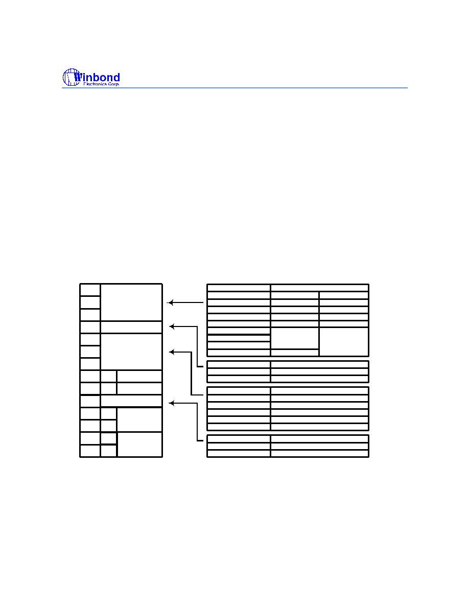
Mode Register Description
The Mode Register designates the operation mode for the read or write cycle. The register is
divided into four fields; (1) Burst Length field sets the length of burst data (2) Addressing Mode
selection bit to designate the column access sequence in a Burst cycle (3) CAS Latency field sets
the access time in clock cycle (4) Single Write Mode selection bit to designate write operation in
burst or single write.
Mode Register Definition
A0
A1
A2
A3
A4
A5
A6
Burst Length
Addressing Mode
CAS Latency
(Test Mode)
A8
Reserved
A0
A7
A0
A9
A0
Write Mode
A10
A0
A11
BS0
"0"
A0
A3
A0
Addressing Mode
A0
0
A0
Sequential
A0
1
A0
Interleave
A0
A9
Single Write Mode
A0
0
A0
Burst read and Burst write
A0
1
A0
Burst read and single write
A0
A2
A1
A0
0
A0
0
1
A0
0
1
0
A0
0
1
A0
1
0
A0
1
0
1
A0
1
0
A0
1
A0
Burst Length
A0
Sequential
A0
Interleave
1
A0
1
A0
2
A0
2
A0
4
A0
4
A0
8
A0
8
A0
Reserved
A0
Reserved
A0
Full Page
A0
CAS Latency
A0
Reserved
A0
Reserved
2
A0
3
Reserved
A0
A6
A5
A4
A0
0
A0
0
1
0
A0
0
1
A0
1
0
A0
0
1
Defines it is a
MRS cycls
Reserved
"0"
BS1
"0"
相关PDF资料 |
PDF描述 |
|---|---|
| W987X6CBG75 | 8M X 16 SYNCHRONOUS DRAM, 5.4 ns, PBGA54 |
| W987Y6CBG80 | 8M X 16 SYNCHRONOUS DRAM, 6 ns, PBGA54 |
| W987Z6CHG75 | 8M X 16 SYNCHRONOUS DRAM, 5.4 ns, PDSO54 |
| W989D2CBJX6E | 16M X 32 DDR DRAM, 5.4 ns, PBGA90 |
| W989D6CBGX7E | 32M X 16 DDR DRAM, 5.4 ns, PBGA54 |
相关代理商/技术参数 |
参数描述 |
|---|---|
| W987Y6CBN | 制造商:未知厂家 制造商全称:未知厂家 功能描述:DRAM |
| W987Z6CBN | 制造商:未知厂家 制造商全称:未知厂家 功能描述:DRAM |
| W988D2FB | 制造商:WINBOND 制造商全称:Winbond 功能描述:256Mb Mobile LPSDR |
| W988D2FBJX6E | 制造商:Winbond Electronics Corp 功能描述:IC LPSDR SDRAM 256MBIT 90VFBGA |
| W988D2FBJX6I | 制造商:WINBOND 制造商全称:Winbond 功能描述:256Mb Mobile LPSDR |
发布紧急采购,3分钟左右您将得到回复。