- 您现在的位置:买卖IC网 > PDF目录69541 > WED9LC6816V1512BI SPECIALTY MEMORY CIRCUIT, PBGA153 PDF资料下载
参数资料
| 型号: | WED9LC6816V1512BI |
| 元件分类: | 存储器 |
| 英文描述: | SPECIALTY MEMORY CIRCUIT, PBGA153 |
| 封装: | MO-163, BGA-153 |
| 文件页数: | 27/27页 |
| 文件大小: | 370K |
| 代理商: | WED9LC6816V1512BI |
第1页第2页第3页第4页第5页第6页第7页第8页第9页第10页第11页第12页第13页第14页第15页第16页第17页第18页第19页第20页第21页第22页第23页第24页第25页第26页当前第27页
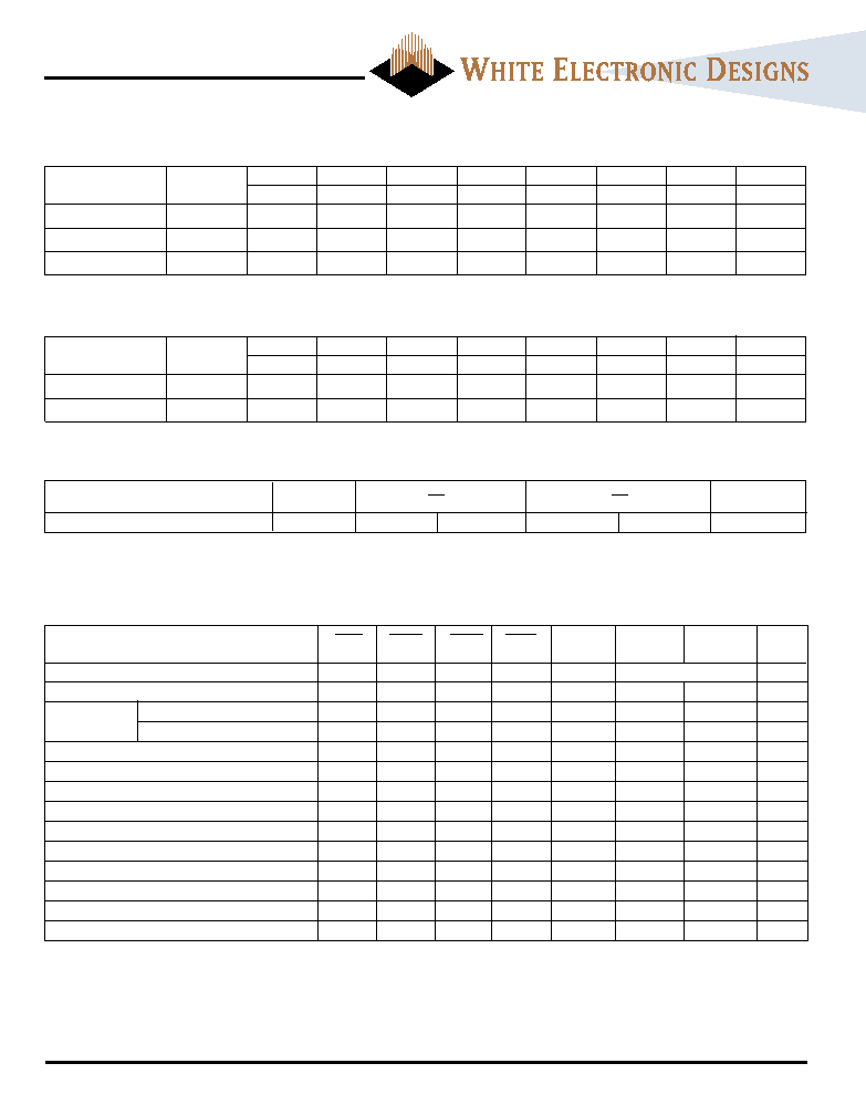
9
White Electronic Designs Corporation (508) 366-5151 www.whiteedc.com
WED9LC6816V
January 2001
Mode Register Set
L
X
OP CODE
Auto Refresh (CBR)
L
H
X
Precharge
Single Bank
L
H
L
X
BA
L
2
Precharge all Banks
L
H
L
X
H
Bank Activate
L
H
X
BA
Row Address
2
Write
L
H
L
X
BA
L
2
Write with Auto Precharge
L
H
L
X
BA
H
2
Read
L
H
L
X
BA
L
2
Read with Auto Precharge
L
H
L
H
X
BA
H
2
Burst Termination
L
H
L
X
3
No Operation
L
H
X
Device Deselect
H
X
Data Write/Output Disable
X
L
X
4
Data Mask/Output Disable
X
H
X
4
NOTES:
1. All of the SDRAM operations are defined by states of SDCE\, SDWE\, SDRAS\, SDCAS\, and BWE0-3 at the positive rising edge of the clock.
2. Bank Select (BA), if A12 (BA0) and A13 (BA1) select between different banks.
3. During a Burst Write cycle there is a zero clock delay, for a Burst Read cycle the delay is equal to the CAS latency.
4. The BWE has two functions for the data DQ Read and Write operations. During a Read cycle, when BWE goes high at a clock timing the data outputs are disabled
and become high impedance after a two clock delay. BWE also provides a data mask function for Write cycles. When it activates, the Write operation at the clock is
prohibited (zero clock latency).
Function
SDCE
SDRAS
SDCAS
SDWE
BWE
A12, A13
SDA10
Notes
A11-0
SDRAM COMMAND TRUTH TABLE
CLOCK FREQUENCY AND LATENCY PARAMETERS - 125MHz SDRAM
(Unit = number of clock)
Frequency
CAS
tRC
tRAS
tRP
tRRD
tRCD
tCCD
tCDL
tRDL
70ns
50ns
20ns
10ns
125MHz (8.0ns)
3
9
6
3
2
3
1
100MHz (10.0ns)
3
7
5
2
1
83MHz (12.0ns)
2
6
4
2
1
Latency
CLOCK FREQUENCY AND LATENCY PARAMETERS - 100MHz SDRAM
(Unit = number of clock)
Frequency
CAS
tRC
tRAS
tRP
tRRD
tRCD
tCCD
tCDL
tRDL
70ns
50ns
20ns
10ns
100MHz (12.0ns)
3
7
5
2
1
83MHz (12.0ns)
2
6
5
2
1
Latency
-10
-12
Parameter
Symbol
Min
Max
Min
Max
Units
Refresh Period (1,2)
tREF
—64
—
64
ms
NOTES:
1. 4096 cycles
2. Any time that the Refresh Period has been exceeded, a minimum of two Auto (CBR) Refresh commands must be given to "wake-up" the device.
REFRESH CYCLE PARAMETERS
相关PDF资料 |
PDF描述 |
|---|---|
| WS128K32-35G2TMEA | 128K X 32 MULTI DEVICE SRAM MODULE, 35 ns, CQFP68 |
| WS128K32-55G2TIE | 128K X 32 MULTI DEVICE SRAM MODULE, 55 ns, CQFP68 |
| WS128K32-35G2TIE | 128K X 32 MULTI DEVICE SRAM MODULE, 35 ns, CQFP68 |
| WS128K32-45G2TIE | 128K X 32 MULTI DEVICE SRAM MODULE, 45 ns, CQFP68 |
| WS512K32-120CJC | 512K X 8 MULTI DEVICE SRAM MODULE, 120 ns, CQCC68 |
相关代理商/技术参数 |
参数描述 |
|---|---|
| WED9LC6816V1610BC | 制造商:未知厂家 制造商全称:未知厂家 功能描述:256K X 32 SSRAM/ 4M X 32 SDRAM |
| WED9LC6816V1610BI | 制造商:White Electronic Designs 功能描述:Res Thin Film 2010 196 Ohm 0.25% 1/4W ±10ppm/°C Molded SMD Plastic T/R 制造商:White Electronic Designs 功能描述:256KX32 SSRAM/ 4MX32 SDRAM |
| WED9LC6816V1612BC | 制造商:未知厂家 制造商全称:未知厂家 功能描述:256K X 32 SSRAM/ 4M X 32 SDRAM |
| WED9LC6816V1612BI | 制造商:未知厂家 制造商全称:未知厂家 功能描述:256K X 32 SSRAM/ 4M X 32 SDRAM |
| WED9LC6816V2010BC | 制造商:未知厂家 制造商全称:未知厂家 功能描述:256K X 32 SSRAM/ 4M X 32 SDRAM |
发布紧急采购,3分钟左右您将得到回复。