参数资料
| 型号: | X98017L128-3.3-Z |
| 厂商: | Intersil |
| 文件页数: | 23/29页 |
| 文件大小: | 0K |
| 描述: | IC VIDEO DIGITIZER TRPL 128MQFP |
| 标准包装: | 66 |
| 类型: | 视频数字转换器,3 通道 AFE |
| 应用: | LCD 电视机/监控器 |
| 安装类型: | 表面贴装 |
| 封装/外壳: | 128-BFQFP |
| 供应商设备封装: | 128-MQFP(14x20) |
| 包装: | 托盘 |
| 产品目录页面: | 1247 (CN2011-ZH PDF) |
第1页第2页第3页第4页第5页第6页第7页第8页第9页第10页第11页第12页第13页第14页第15页第16页第17页第18页第19页第20页第21页第22页当前第23页第24页第25页第26页第27页第28页第29页
3
FN8218.3
March 8, 2006
T
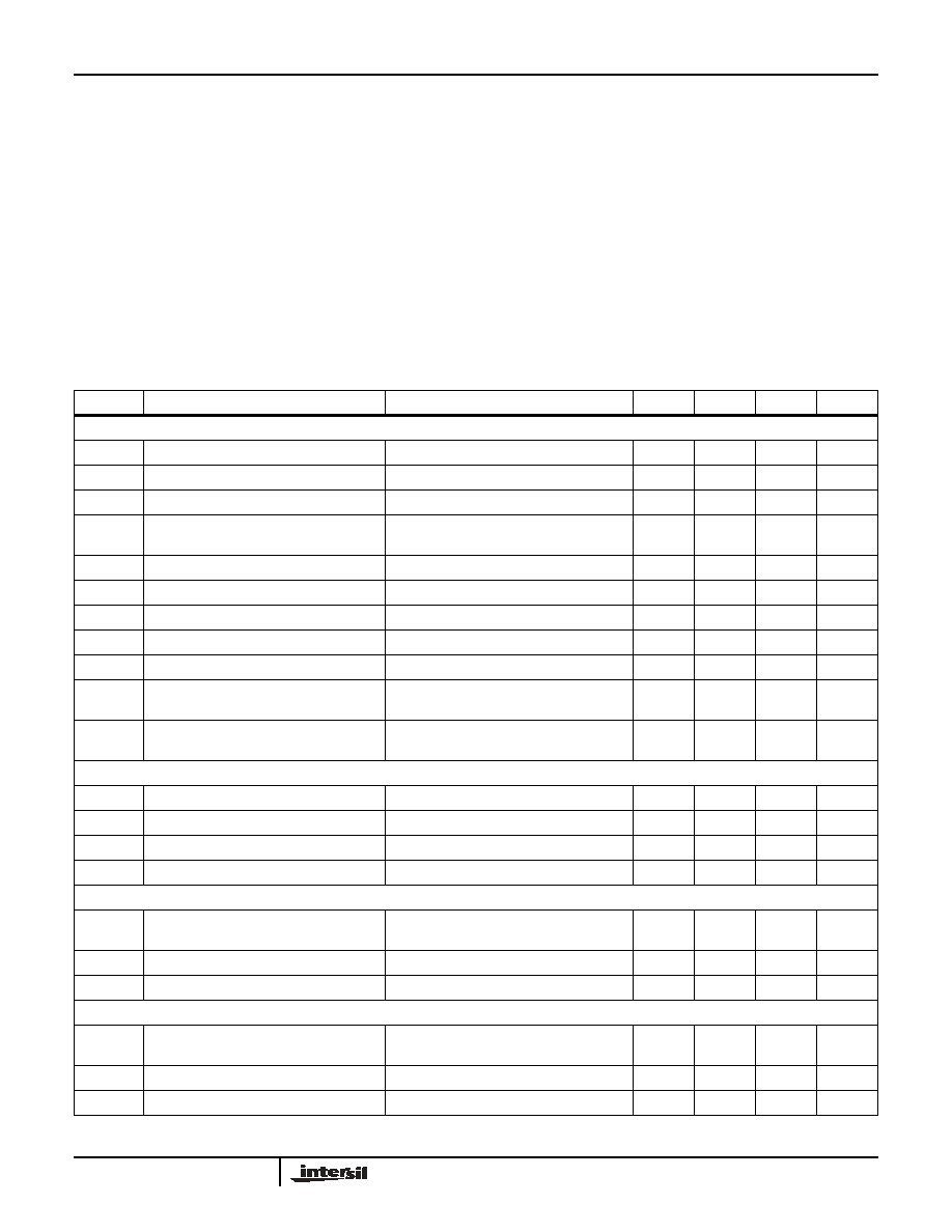
Absolute Maximum Ratings
Recommended Operating Conditions
Voltage on VA, VD, or VX
(referenced to GNDA=GNDD=GNDX) . . . . . . . . . . . . . . . . . . . 4.0V
Voltage on any analog input pin
(referenced to GNDA) . . . . . . . . . . . . . . . . . . . . . . . . . . -0.3V to VA
Voltage on any digital input pin
(referenced to GNDD) . . . . . . . . . . . . . . . . . . . . . . . -0.3V to +6.0V
Current into any output pin
. . . . . . . . . . . . . . . . . . . . . . . . . . . . . .±20mA
Operating Temperature range . . . . . . . . . . . . . . . . . . . . . 0
°C to +70°C
Junction Temperature . . . . . . . . . . . . . . . . . . . . . . . . . . . . . . +125
°C
Storage Temperature. . . . . . . . . . . . . . . . . . . . . . . .-65
°C to +150°C
Temperature (Commercial) . . . . . . . . . . . . . . . . . . . . . 0°C to +70°C
Supply Voltage. . . . . . . . . . . . . . . . . . . . . . . . . VA = VD = VX = 3.3V
CAUTION: Stresses above those listed under “Absolute Maximum Ratings” may cause permanent damage to the device. This is a stress rating only; functional
operation of the device (at these or any other conditions above those listed in the operational sections of this specification) is not implied. Exposure to absolute
maximum rating conditions for extended periods may affect device reliability.
Electrical Specifications
Specifications apply for VA = VD = VX = 3.3V, pixel rate = 170MHz, fXTAL = 25MHz, TA = 25°C,
unless otherwise noted
SYMBOL
PARAMETER
COMMENT
MIN
TYP
MAX
UNIT
FULL CHANNEL CHARACTERISTICS
ADC Resolution
8Bits
Missing Codes
Guaranteed monotonic
None
Conversion Rate
Per Channel
10
170
MHz
DNL
Differential Non-Linearity
±0.5
+1.0
-0.9
LSB
INL
Integral Non-Linearity
±1.1
±3.25
LSB
Gain Adjustment Range
±6
dB
Gain Adjustment Resolution
8Bits
Gain Matching Between Channels
Percent of full scale
±1
%
Full Channel Offset Error, ABLC enabled ADC LSBs, over time and temperature
±0.125
±0.5
LSB
Offset Adjustment Range, ABLC
enabled or disabled
ADC LSBs (see ABLC applications
information section)
±127
LSB
Overvoltage Recovery Time
For 150% overrange, maximum bandwidth
setting
5ns
ANALOG VIDEO INPUT CHARACTERISTICS (RIN1, GIN1, BIN1, RIN2, GIN2, BIN2)
Input Range
0.35
0.7
1.4
VP-P
Input Bias Current
DC restore clamp off
±0.01
±1
A
Input Capacitance
5pF
Full Power Bandwidth
Programmable
780
MHz
INPUT CHARACTERISTICS (SOGIN1, SOGIN2)
VIH/VIL
Input Threshold Voltage
Programmable - See Register Listing for
Details
0 to
-0.3
V
Hysteresis
Centered around threshold voltage
40
mV
Input capacitance
5pF
INPUT CHARACTERISTICS (HSYNCIN1, HSYNCIN2)
VIH/VIL
Input Threshold Voltage
Programmable - See Register Listing for
Details
0.4 to 3.2
V
Hysteresis
Centered around threshold voltage
240
mV
RIN
Input impedance
1.2
k
X98017
相关PDF资料 |
PDF描述 |
|---|---|
| X98021L128-3.3-Z | IC TRPL VID DIGITIZER 128MQFP |
| X98024L128-3.3-Z | IC TRPL VID DIGITIZER 128MQFP |
| X98027L128-3.3-Z | IC TRPL VID DIGITIZER 128MQFP |
| XC25BS5001MR-G | IC CLK BUFFER PLL SOT26 |
| XC25BS7001ER-G | IC CLK GENERATOR PLL USP-6C |
相关代理商/技术参数 |
参数描述 |
|---|---|
| X98021 | 制造商:INTERSIL 制造商全称:Intersil Corporation 功能描述:210MHz Triple Video Digitizer with Digital PLL |
| X98021_06 | 制造商:INTERSIL 制造商全称:Intersil Corporation 功能描述:210MHz Triple Video Digitizer with Digital PLL |
| X98021EVAL | 制造商:Intersil Corporation 功能描述:EVALUATION BOARD FOR X98021 - Bulk |
| X98021L128-3.3 | 制造商:INTERSIL 制造商全称:Intersil Corporation 功能描述:210MHz Triple Video Digitizer with Digital PLL |
| X98021L128-3.3-Z | 功能描述:IC TRPL VID DIGITIZER 128MQFP RoHS:是 类别:集成电路 (IC) >> 线性 - 视频处理 系列:- 标准包装:250 系列:- 类型:电平移位器 应用:LCD 电视机/监控器 安装类型:表面贴装 封装/外壳:28-WFQFN 裸露焊盘 供应商设备封装:28-WQFN(4x4)裸露焊盘 包装:带卷 (TR) 其它名称:296-32523-2TPS65198RUYT-ND |
发布紧急采购,3分钟左右您将得到回复。