参数资料
| 型号: | XC2S100-5TQ144C |
| 厂商: | Xilinx Inc |
| 文件页数: | 13/99页 |
| 文件大小: | 0K |
| 描述: | IC FPGA 2.5V 600 CLB'S 144-TQFP |
| 标准包装: | 60 |
| 系列: | Spartan®-II |
| LAB/CLB数: | 600 |
| 逻辑元件/单元数: | 2700 |
| RAM 位总计: | 40960 |
| 输入/输出数: | 92 |
| 门数: | 100000 |
| 电源电压: | 2.375 V ~ 2.625 V |
| 安装类型: | 表面贴装 |
| 工作温度: | 0°C ~ 85°C |
| 封装/外壳: | 144-LQFP |
| 供应商设备封装: | 144-TQFP(20x20) |
| 其它名称: | 122-1229 XC2S100-5TQ144C-ND |
第1页第2页第3页第4页第5页第6页第7页第8页第9页第10页第11页第12页当前第13页第14页第15页第16页第17页第18页第19页第20页第21页第22页第23页第24页第25页第26页第27页第28页第29页第30页第31页第32页第33页第34页第35页第36页第37页第38页第39页第40页第41页第42页第43页第44页第45页第46页第47页第48页第49页第50页第51页第52页第53页第54页第55页第56页第57页第58页第59页第60页第61页第62页第63页第64页第65页第66页第67页第68页第69页第70页第71页第72页第73页第74页第75页第76页第77页第78页第79页第80页第81页第82页第83页第84页第85页第86页第87页第88页第89页第90页第91页第92页第93页第94页第95页第96页第97页第98页第99页
Spartan-II FPGA Family: Functional Description
DS001-2 (v2.8) June 13, 2008
Module 2 of 4
Product Specification
20
R
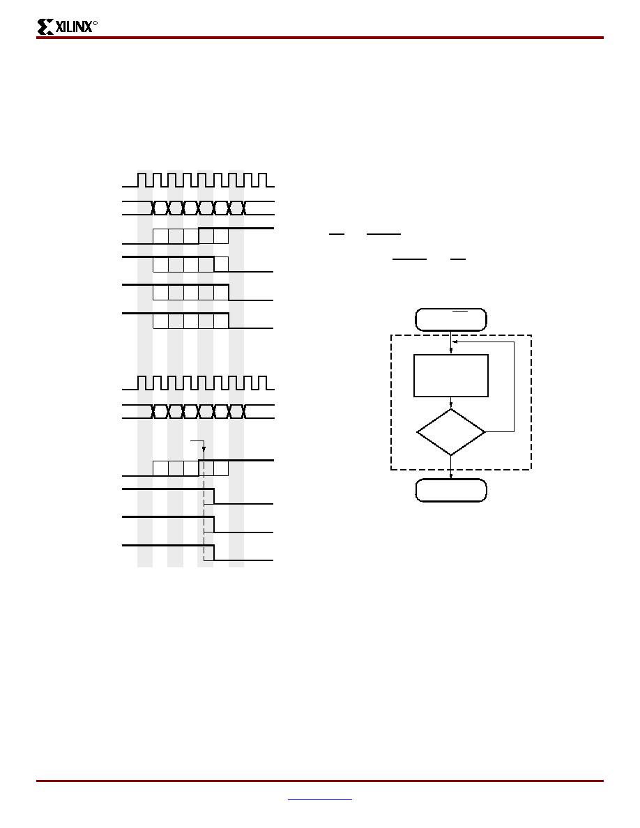
By default, these operations are synchronized to CCLK.
The entire start-up sequence lasts eight cycles, called
C0-C7, after which the loaded design is fully functional. The
default timing for start-up is shown in the top half of
Figure 13. The four operations can be selected to switch on
any CCLK cycle C1-C6 through settings in the Xilinx
software. Heavy lines show default settings.
The bottom half of Figure 13 shows another commonly
used version of the start-up timing known as
Sync-to-DONE. This version makes the GTS, GSR, and
GWE events conditional upon the DONE pin going High.
This timing is important for a daisy chain of multiple FPGAs
in serial mode, since it ensures that all FPGAs go through
start-up together, after all their DONE pins have gone High.
Sync-to-DONE timing is selected by setting the GTS, GSR,
and GWE cycles to a value of DONE in the configuration
options. This causes these signals to transition one clock
cycle after DONE externally transitions High.
Serial Modes
There are two serial configuration modes: In Master Serial
mode, the FPGA controls the configuration process by
driving CCLK as an output. In Slave Serial mode, the FPGA
passively receives CCLK as an input from an external agent
(e.g., a microprocessor, CPLD, or second FPGA in master
mode) that is controlling the configuration process. In both
modes, the FPGA is configured by loading one bit per
CCLK cycle. The MSB of each configuration data byte is
always written to the DIN pin first.
See Figure 14 for the sequence for loading data into the
Spartan-II FPGA serially. This is an expansion of the "Load
Configuration Data Frames" block in Figure 11. Note that
CS and WRITE normally are not used during serial
configuration. To ensure successful loading of the FPGA,
do not toggle WRITE with CS Low during serial
configuration.
Figure 13: Start-Up Waveforms
Start-up CLK
Default Cycles
Sync to DONE
01
2
3
4
5
6
7
01
DONE High
23
4
56
7
Phase
Start-up CLK
Phase
DONE
GTS
GSR
GWE
DS001_13_090600
DONE
GTS
GSR
GWE
Figure 14: Loading Serial Mode Configuration Data
DS001_14_042403
No
Yes
End of
Configuration
Data File?
After INIT
Goes High
User Load One
Configuration
Bit on Next
CCLK Rising Edge
To CRC Check
相关PDF资料 |
PDF描述 |
|---|---|
| 24LC22AT-I/SN | IC EEPROM 2KBIT 400KHZ 8SOIC |
| XC3S400A-4FT256C | IC SPARTAN-3A FPGA 400K 256FTBGA |
| XC3S200A-4FG320C | IC SPARTAN-3A FPGA 200K 320FBGA |
| XC2S50E-6PQ208C | IC FPGA 1.8V 384 CLB'S 208-PQFP |
| XC3S200A-4FT256I | IC SPARTAN-3A FPGA 200K 256FTBGA |
相关代理商/技术参数 |
参数描述 |
|---|---|
| XC2S100-5TQ144I | 功能描述:IC FPGA 2.5V I-TEMP 144-TQFP RoHS:否 类别:集成电路 (IC) >> 嵌入式 - FPGA(现场可编程门阵列) 系列:Spartan®-II 标准包装:40 系列:Spartan® 6 LX LAB/CLB数:3411 逻辑元件/单元数:43661 RAM 位总计:2138112 输入/输出数:358 门数:- 电源电压:1.14 V ~ 1.26 V 安装类型:表面贴装 工作温度:-40°C ~ 100°C 封装/外壳:676-BGA 供应商设备封装:676-FBGA(27x27) |
| XC2S100-5TQG144C | 功能描述:IC SPARTAN-II FPGA 100K 144-TQFP RoHS:是 类别:集成电路 (IC) >> 嵌入式 - FPGA(现场可编程门阵列) 系列:Spartan®-II 标准包装:60 系列:XP LAB/CLB数:- 逻辑元件/单元数:10000 RAM 位总计:221184 输入/输出数:244 门数:- 电源电压:1.71 V ~ 3.465 V 安装类型:表面贴装 工作温度:0°C ~ 85°C 封装/外壳:388-BBGA 供应商设备封装:388-FPBGA(23x23) 其它名称:220-1241 |
| XC2S100-5TQG144I | 制造商:Xilinx 功能描述:FPGA SPARTAN-II 100K GATES 2700 CELLS 263MHZ 2.5V 144TQFP EP - Trays 制造商:Xilinx 功能描述:XLXXC2S100-5TQG144I IC SYSTEM GATE |
| XC2S100-5VQ100C | 制造商:XILINX 制造商全称:XILINX 功能描述:Spartan-II 2.5V FPGA Family:Introduction and Ordering Information |
| XC2S100-5VQ100I | 制造商:XILINX 制造商全称:XILINX 功能描述:Spartan-II 2.5V FPGA Family:Introduction and Ordering Information |
发布紧急采购,3分钟左右您将得到回复。