参数资料
| 型号: | XC2S100-5TQ144C |
| 厂商: | Xilinx Inc |
| 文件页数: | 33/99页 |
| 文件大小: | 0K |
| 描述: | IC FPGA 2.5V 600 CLB'S 144-TQFP |
| 标准包装: | 60 |
| 系列: | Spartan®-II |
| LAB/CLB数: | 600 |
| 逻辑元件/单元数: | 2700 |
| RAM 位总计: | 40960 |
| 输入/输出数: | 92 |
| 门数: | 100000 |
| 电源电压: | 2.375 V ~ 2.625 V |
| 安装类型: | 表面贴装 |
| 工作温度: | 0°C ~ 85°C |
| 封装/外壳: | 144-LQFP |
| 供应商设备封装: | 144-TQFP(20x20) |
| 其它名称: | 122-1229 XC2S100-5TQ144C-ND |
第1页第2页第3页第4页第5页第6页第7页第8页第9页第10页第11页第12页第13页第14页第15页第16页第17页第18页第19页第20页第21页第22页第23页第24页第25页第26页第27页第28页第29页第30页第31页第32页当前第33页第34页第35页第36页第37页第38页第39页第40页第41页第42页第43页第44页第45页第46页第47页第48页第49页第50页第51页第52页第53页第54页第55页第56页第57页第58页第59页第60页第61页第62页第63页第64页第65页第66页第67页第68页第69页第70页第71页第72页第73页第74页第75页第76页第77页第78页第79页第80页第81页第82页第83页第84页第85页第86页第87页第88页第89页第90页第91页第92页第93页第94页第95页第96页第97页第98页第99页
Spartan-II FPGA Family: Functional Description
DS001-2 (v2.8) June 13, 2008
Module 2 of 4
Product Specification
39
R
the LOC property is described below. Table 16 summarizes
the input standards compatibility requirements.
An optional delay element is associated with each IBUF.
When the IBUF drives a flip-flop within the IOB, the delay
element by default activates to ensure a zero hold-time
requirement. The NODELAY=TRUE property overrides this
default.
When the IBUF does not drive a flip-flop within the IOB, the
delay element de-activates by default to provide higher
performance. To delay the input signal, activate the delay
element with the DELAY=TRUE property.
IBUFG
Signals used as high fanout clock inputs to the
Spartan-II device should drive a global clock input buffer
(IBUFG) via an external input port in order to take
advantage of one of the four dedicated global clock
distribution networks. The output of the IBUFG primitive can
only drive a CLKDLL, CLKDLLHF, or a BUFG primitive. The
generic IBUFG primitive appears in Figure 37.
With no extension or property specified for the generic
IBUFG primitive, the assumed standard is LVTTL.
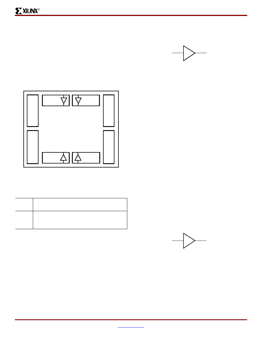
The voltage reference signal is "banked" within the
Spartan-II device on a half-edge basis such that for all
packages there are eight independent VREF banks
internally. See Figure 36 for a representation of the I/O
banks. Within each bank approximately one of every six I/O
pins is automatically configured as a VREF input.
IBUFG placement restrictions require any differential
amplifier input signals within a bank be of the same
standard. The LOC property can specify a location for the
IBUFG.
As an added convenience, the BUFGP can be used to
instantiate a high fanout clock input. The BUFGP primitive
represents a combination of the LVTTL IBUFG and BUFG
primitives, such that the output of the BUFGP can connect
directly to the clock pins throughout the design.
The Spartan-II FPGA BUFGP primitive can only be placed
in a global clock pad location. The LOC property can specify
a location for the BUFGP.
OBUF
An OBUF must drive outputs through an external output
port. The generic output buffer (OBUF) primitive appears in
With no extension or property specified for the generic
OBUF primitive, the assumed standard is slew rate limited
LVTTL with 12 mA drive strength.
The LVTTL OBUF additionally can support one of two slew
rate modes to minimize bus transients. By default, the slew
rate for each output buffer is reduced to minimize power bus
transients when switching non-critical signals.
Figure 36: I/O Banks
Table 16: Xilinx Input Standards Compatibility
Requirements
Rule 1
All differential amplifier input signals within a
bank are required to be of the same standard.
Rule 2
There are no placement restrictions for inputs
with standards that require a single-ended input
buffer.
DS001_03_060100
Bank 0
GCLK3
GCLK2
GCLK1
GCLK0
Bank 1
Bank 5
Bank 4
Spartan-II
Device
Bank
7
Bank
6
Bank
2
Bank
3
Figure 37: Global Clock Input Buffer (IBUFG) Primitive
Figure 38: Output Buffer (OBUF) Primitive
O
I
IBUFG
DS001_37_061200
O
I
OBUF
DS001_38_061200
相关PDF资料 |
PDF描述 |
|---|---|
| 24LC22AT-I/SN | IC EEPROM 2KBIT 400KHZ 8SOIC |
| XC3S400A-4FT256C | IC SPARTAN-3A FPGA 400K 256FTBGA |
| XC3S200A-4FG320C | IC SPARTAN-3A FPGA 200K 320FBGA |
| XC2S50E-6PQ208C | IC FPGA 1.8V 384 CLB'S 208-PQFP |
| XC3S200A-4FT256I | IC SPARTAN-3A FPGA 200K 256FTBGA |
相关代理商/技术参数 |
参数描述 |
|---|---|
| XC2S100-5TQ144I | 功能描述:IC FPGA 2.5V I-TEMP 144-TQFP RoHS:否 类别:集成电路 (IC) >> 嵌入式 - FPGA(现场可编程门阵列) 系列:Spartan®-II 标准包装:40 系列:Spartan® 6 LX LAB/CLB数:3411 逻辑元件/单元数:43661 RAM 位总计:2138112 输入/输出数:358 门数:- 电源电压:1.14 V ~ 1.26 V 安装类型:表面贴装 工作温度:-40°C ~ 100°C 封装/外壳:676-BGA 供应商设备封装:676-FBGA(27x27) |
| XC2S100-5TQG144C | 功能描述:IC SPARTAN-II FPGA 100K 144-TQFP RoHS:是 类别:集成电路 (IC) >> 嵌入式 - FPGA(现场可编程门阵列) 系列:Spartan®-II 标准包装:60 系列:XP LAB/CLB数:- 逻辑元件/单元数:10000 RAM 位总计:221184 输入/输出数:244 门数:- 电源电压:1.71 V ~ 3.465 V 安装类型:表面贴装 工作温度:0°C ~ 85°C 封装/外壳:388-BBGA 供应商设备封装:388-FPBGA(23x23) 其它名称:220-1241 |
| XC2S100-5TQG144I | 制造商:Xilinx 功能描述:FPGA SPARTAN-II 100K GATES 2700 CELLS 263MHZ 2.5V 144TQFP EP - Trays 制造商:Xilinx 功能描述:XLXXC2S100-5TQG144I IC SYSTEM GATE |
| XC2S100-5VQ100C | 制造商:XILINX 制造商全称:XILINX 功能描述:Spartan-II 2.5V FPGA Family:Introduction and Ordering Information |
| XC2S100-5VQ100I | 制造商:XILINX 制造商全称:XILINX 功能描述:Spartan-II 2.5V FPGA Family:Introduction and Ordering Information |
发布紧急采购,3分钟左右您将得到回复。