参数资料
| 型号: | XC2S100-5TQ144C |
| 厂商: | Xilinx Inc |
| 文件页数: | 32/99页 |
| 文件大小: | 0K |
| 描述: | IC FPGA 2.5V 600 CLB'S 144-TQFP |
| 标准包装: | 60 |
| 系列: | Spartan®-II |
| LAB/CLB数: | 600 |
| 逻辑元件/单元数: | 2700 |
| RAM 位总计: | 40960 |
| 输入/输出数: | 92 |
| 门数: | 100000 |
| 电源电压: | 2.375 V ~ 2.625 V |
| 安装类型: | 表面贴装 |
| 工作温度: | 0°C ~ 85°C |
| 封装/外壳: | 144-LQFP |
| 供应商设备封装: | 144-TQFP(20x20) |
| 其它名称: | 122-1229 XC2S100-5TQ144C-ND |
第1页第2页第3页第4页第5页第6页第7页第8页第9页第10页第11页第12页第13页第14页第15页第16页第17页第18页第19页第20页第21页第22页第23页第24页第25页第26页第27页第28页第29页第30页第31页当前第32页第33页第34页第35页第36页第37页第38页第39页第40页第41页第42页第43页第44页第45页第46页第47页第48页第49页第50页第51页第52页第53页第54页第55页第56页第57页第58页第59页第60页第61页第62页第63页第64页第65页第66页第67页第68页第69页第70页第71页第72页第73页第74页第75页第76页第77页第78页第79页第80页第81页第82页第83页第84页第85页第86页第87页第88页第89页第90页第91页第92页第93页第94页第95页第96页第97页第98页第99页
Spartan-II FPGA Family: Functional Description
DS001-2 (v2.8) June 13, 2008
Module 2 of 4
Product Specification
38
R
PCI — Peripheral Component Interface
The Peripheral Component Interface (PCI) standard
specifies support for both 33 MHz and 66 MHz PCI bus
applications. It uses a LVTTL input buffer and a push-pull
output buffer. This standard does not require the use of a
reference voltage (VREF) or a board termination voltage
(VTT), however, it does require a 3.3V output source voltage
(VCCO). I/Os configured for the PCI, 33 MHz, 5V standard
are also 5V-tolerant.
GTL — Gunning Transceiver Logic Terminated
The Gunning Transceiver Logic (GTL) standard is a
high-speed bus standard (JESD8.3). Xilinx has
implemented the terminated variation of this standard. This
standard requires a differential amplifier input buffer and an
open-drain output buffer.
GTL+ — Gunning Transceiver Logic Plus
The Gunning Transceiver Logic Plus (GTL+) standard is a
high-speed bus standard (JESD8.3).
HSTL — High-Speed Transceiver Logic
The High-Speed Transceiver Logic (HSTL) standard is a
general purpose high-speed, 1.5V bus standard (EIA/JESD
8-6). This standard has four variations or classes. Versatile
I/O devices support Class I, III, and IV. This standard
requires a Differential Amplifier input buffer and a Push-Pull
output buffer.
SSTL3 — Stub Series Terminated Logic for 3.3V
The Stub Series Terminated Logic for 3.3V (SSTL3)
standard is a general purpose 3.3V memory bus standard
(JESD8-8). This standard has two classes, I and II.
Versatile I/O devices support both classes for the SSTL3
standard. This standard requires a Differential Amplifier
input buffer and an Push-Pull output buffer.
SSTL2 — Stub Series Terminated Logic for 2.5V
The Stub Series Terminated Logic for 2.5V (SSTL2)
standard is a general purpose 2.5V memory bus standard
(JESD8-9). This standard has two classes, I and II.
Versatile I/O devices support both classes for the SSTL2
standard. This standard requires a Differential Amplifier
input buffer and an Push-Pull output buffer.
CTT — Center Tap Terminated
The Center Tap Terminated (CTT) standard is a 3.3V
memory bus standard (JESD8-4). This standard requires a
Differential Amplifier input buffer and a Push-Pull output
buffer.
AGP-2X — Advanced Graphics Port
The AGP standard is a 3.3V Advanced Graphics Port-2X
bus standard used with processors for graphics
applications. This standard requires a Push-Pull output
buffer and a Differential Amplifier input buffer.
Library Primitives
The Xilinx library includes an extensive list of primitives
designed to provide support for the variety of Versatile I/O
features. Most of these primitives represent variations of the
five generic Versatile I/O primitives:
IBUF (input buffer)
IBUFG (global clock input buffer)
OBUF (output buffer)
OBUFT (3-state output buffer)
IOBUF (input/output buffer)
These primitives are available with various extensions to
define the desired I/O standard. However, it is
recommended that customers use a a property or attribute
on the generic primitive to specify the I/O standard. See
IBUF
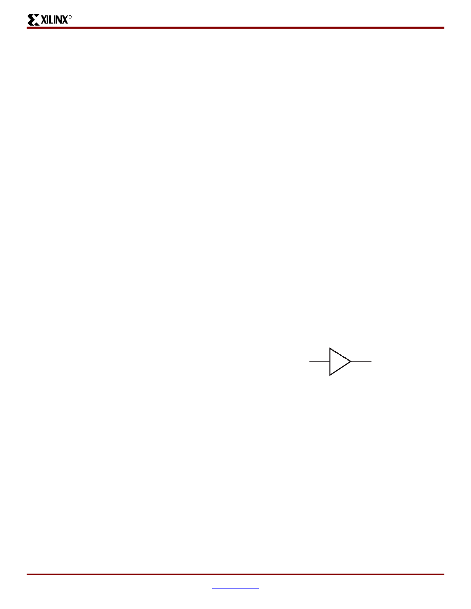
Signals used as inputs to the Spartan-II device must source
an input buffer (IBUF) via an external input port. The generic
IBUF primitive appears in Figure 35. The assumed standard
is LVTTL when the generic IBUF has no specified extension
or property.
When the IBUF primitive supports an I/O standard such as
LVTTL, LVCMOS, or PCI33_5, the IBUF automatically
configures as a 5V tolerant input buffer unless the VCCO for
the bank is less than 2V. If the single-ended IBUF is placed
in a bank with an HSTL standard (VCCO < 2V), the input
buffer is not 5V tolerant.
The voltage reference signal is "banked" within the
Spartan-II device on a half-edge basis such that for all
packages there are eight independent VREF banks
internally. See Figure 36 for a representation of the I/O
banks. Within each bank approximately one of every six I/O
pins is automatically configured as a VREF input.
IBUF placement restrictions require that any differential
amplifier input signals within a bank be of the same
standard. How to specify a specific location for the IBUF via
Figure 35: Input Buffer (IBUF) Primitive
O
I
IBUF
DS001_35_061200
相关PDF资料 |
PDF描述 |
|---|---|
| 24LC22AT-I/SN | IC EEPROM 2KBIT 400KHZ 8SOIC |
| XC3S400A-4FT256C | IC SPARTAN-3A FPGA 400K 256FTBGA |
| XC3S200A-4FG320C | IC SPARTAN-3A FPGA 200K 320FBGA |
| XC2S50E-6PQ208C | IC FPGA 1.8V 384 CLB'S 208-PQFP |
| XC3S200A-4FT256I | IC SPARTAN-3A FPGA 200K 256FTBGA |
相关代理商/技术参数 |
参数描述 |
|---|---|
| XC2S100-5TQ144I | 功能描述:IC FPGA 2.5V I-TEMP 144-TQFP RoHS:否 类别:集成电路 (IC) >> 嵌入式 - FPGA(现场可编程门阵列) 系列:Spartan®-II 标准包装:40 系列:Spartan® 6 LX LAB/CLB数:3411 逻辑元件/单元数:43661 RAM 位总计:2138112 输入/输出数:358 门数:- 电源电压:1.14 V ~ 1.26 V 安装类型:表面贴装 工作温度:-40°C ~ 100°C 封装/外壳:676-BGA 供应商设备封装:676-FBGA(27x27) |
| XC2S100-5TQG144C | 功能描述:IC SPARTAN-II FPGA 100K 144-TQFP RoHS:是 类别:集成电路 (IC) >> 嵌入式 - FPGA(现场可编程门阵列) 系列:Spartan®-II 标准包装:60 系列:XP LAB/CLB数:- 逻辑元件/单元数:10000 RAM 位总计:221184 输入/输出数:244 门数:- 电源电压:1.71 V ~ 3.465 V 安装类型:表面贴装 工作温度:0°C ~ 85°C 封装/外壳:388-BBGA 供应商设备封装:388-FPBGA(23x23) 其它名称:220-1241 |
| XC2S100-5TQG144I | 制造商:Xilinx 功能描述:FPGA SPARTAN-II 100K GATES 2700 CELLS 263MHZ 2.5V 144TQFP EP - Trays 制造商:Xilinx 功能描述:XLXXC2S100-5TQG144I IC SYSTEM GATE |
| XC2S100-5VQ100C | 制造商:XILINX 制造商全称:XILINX 功能描述:Spartan-II 2.5V FPGA Family:Introduction and Ordering Information |
| XC2S100-5VQ100I | 制造商:XILINX 制造商全称:XILINX 功能描述:Spartan-II 2.5V FPGA Family:Introduction and Ordering Information |
发布紧急采购,3分钟左右您将得到回复。