参数资料
| 型号: | XC2S100-5TQ144C |
| 厂商: | Xilinx Inc |
| 文件页数: | 22/99页 |
| 文件大小: | 0K |
| 描述: | IC FPGA 2.5V 600 CLB'S 144-TQFP |
| 标准包装: | 60 |
| 系列: | Spartan®-II |
| LAB/CLB数: | 600 |
| 逻辑元件/单元数: | 2700 |
| RAM 位总计: | 40960 |
| 输入/输出数: | 92 |
| 门数: | 100000 |
| 电源电压: | 2.375 V ~ 2.625 V |
| 安装类型: | 表面贴装 |
| 工作温度: | 0°C ~ 85°C |
| 封装/外壳: | 144-LQFP |
| 供应商设备封装: | 144-TQFP(20x20) |
| 其它名称: | 122-1229 XC2S100-5TQ144C-ND |
第1页第2页第3页第4页第5页第6页第7页第8页第9页第10页第11页第12页第13页第14页第15页第16页第17页第18页第19页第20页第21页当前第22页第23页第24页第25页第26页第27页第28页第29页第30页第31页第32页第33页第34页第35页第36页第37页第38页第39页第40页第41页第42页第43页第44页第45页第46页第47页第48页第49页第50页第51页第52页第53页第54页第55页第56页第57页第58页第59页第60页第61页第62页第63页第64页第65页第66页第67页第68页第69页第70页第71页第72页第73页第74页第75页第76页第77页第78页第79页第80页第81页第82页第83页第84页第85页第86页第87页第88页第89页第90页第91页第92页第93页第94页第95页第96页第97页第98页第99页
Spartan-II FPGA Family: Functional Description
DS001-2 (v2.8) June 13, 2008
Module 2 of 4
Product Specification
29
R
division factor N except for non-integer division in High
Frequency (HF) mode. For division factor 1.5 the duty cycle
in the HF mode is 33.3% High and 66.7% Low. For division
factor 2.5, the duty cycle in the HF mode is 40.0% High and
60.0% Low.
1x Clock Outputs — CLK[0|90|180|270]
The 1x clock output pin CLK0 represents a
delay-compensated version of the source clock (CLKIN)
signal. The CLKDLL primitive provides three phase-shifted
versions of the CLK0 signal while CLKDLLHF provides only
the 180 degree phase-shifted version. The relationship
between phase shift and the corresponding period shift
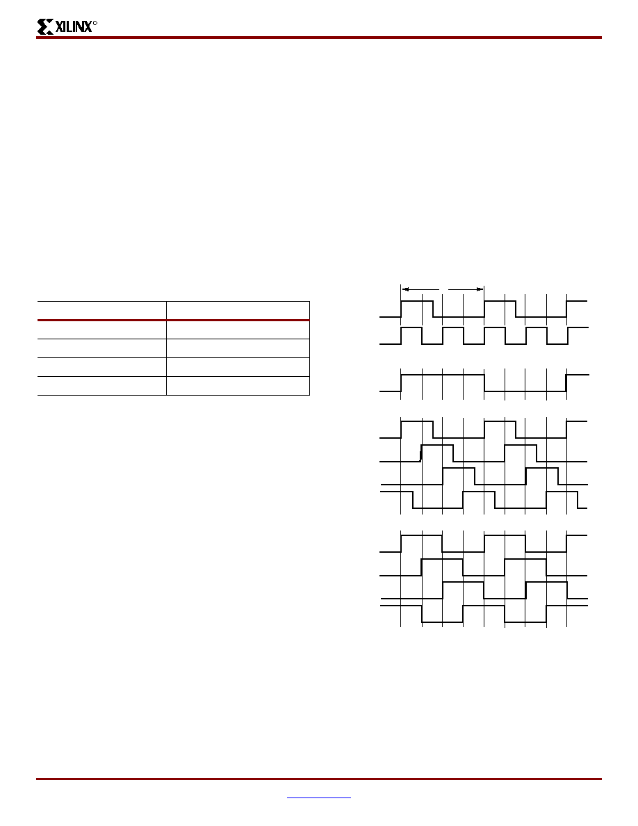
appears in Table 10.
The timing diagrams in Figure 26 illustrate the DLL clock
output characteristics.
The DLL provides duty cycle correction on all 1x clock
outputs such that all 1x clock outputs by default have a
50/50 duty cycle. The DUTY_CYCLE_CORRECTION
property (TRUE by default), controls this feature. In order to
deactivate the DLL duty cycle correction, attach the
DUTY_CYCLE_CORRECTION=FALSE property to the
DLL primitive. When duty cycle correction deactivates, the
output clock has the same duty cycle as the source clock.
The DLL clock outputs can drive an OBUF, a BUFG, or they
can route directly to destination clock pins. The DLL clock
outputs can only drive the BUFGs that reside on the same
edge (top or bottom).
Locked Output — LOCKED
In order to achieve lock, the DLL may need to sample
several thousand clock cycles. After the DLL achieves lock
the LOCKED signal activates. The "DLL Timing
Parameters" section of Module 3 provides estimates for
locking times.
In order to guarantee that the system clock is established
prior to the device "waking up," the DLL can delay the
completion of the device configuration process until after
the DLL locks. The STARTUP_WAIT property activates this
feature.
Until the LOCKED signal activates, the DLL output clocks
are not valid and can exhibit glitches, spikes, or other
spurious movement. In particular the CLK2X output will
appear as a 1x clock with a 25/75 duty cycle.
DLL Properties
Properties provide access to some of the Spartan-II family
DLL features, (for example, clock division and duty cycle
correction).
Duty Cycle Correction Property
The 1x clock outputs, CLK0, CLK90, CLK180, and CLK270,
use the duty-cycle corrected default, such that they exhibit a
50/50 duty cycle. The DUTY_CYCLE_CORRECTION
property (by default TRUE) controls this feature. To
deactivate the DLL duty-cycle correction for the 1x clock
outputs, attach the DUTY_CYCLE_CORRECTION=FALSE
property to the DLL primitive.
Clock Divide Property
The CLKDV_DIVIDE property specifies how the signal on
the CLKDV pin is frequency divided with respect to the
CLK0 pin. The values allowed for this property are 1.5, 2,
2.5, 3, 4, 5, 8, or 16; the default value is 2.
Table 10: Relationship of Phase-Shifted Output Clock
to Period Shift
Phase (degrees)
Period Shift (percent)
00%
90
25%
180
50%
270
75%
Figure 26: DLL Output Characteristics
DS001_26_032300
CLKIN
CLK2X
CLK0
CLK90
CLK180
CLK270
CLKDV
CLKDV_DIVIDE = 2
DUTY_CYCLE_CORRECTION = FALSE
CLK0
CLK90
CLK180
CLK270
DUTY_CYCLE_CORRECTION = TRUE
T
0
90 180 270
0
90 180 270
相关PDF资料 |
PDF描述 |
|---|---|
| 24LC22AT-I/SN | IC EEPROM 2KBIT 400KHZ 8SOIC |
| XC3S400A-4FT256C | IC SPARTAN-3A FPGA 400K 256FTBGA |
| XC3S200A-4FG320C | IC SPARTAN-3A FPGA 200K 320FBGA |
| XC2S50E-6PQ208C | IC FPGA 1.8V 384 CLB'S 208-PQFP |
| XC3S200A-4FT256I | IC SPARTAN-3A FPGA 200K 256FTBGA |
相关代理商/技术参数 |
参数描述 |
|---|---|
| XC2S100-5TQ144I | 功能描述:IC FPGA 2.5V I-TEMP 144-TQFP RoHS:否 类别:集成电路 (IC) >> 嵌入式 - FPGA(现场可编程门阵列) 系列:Spartan®-II 标准包装:40 系列:Spartan® 6 LX LAB/CLB数:3411 逻辑元件/单元数:43661 RAM 位总计:2138112 输入/输出数:358 门数:- 电源电压:1.14 V ~ 1.26 V 安装类型:表面贴装 工作温度:-40°C ~ 100°C 封装/外壳:676-BGA 供应商设备封装:676-FBGA(27x27) |
| XC2S100-5TQG144C | 功能描述:IC SPARTAN-II FPGA 100K 144-TQFP RoHS:是 类别:集成电路 (IC) >> 嵌入式 - FPGA(现场可编程门阵列) 系列:Spartan®-II 标准包装:60 系列:XP LAB/CLB数:- 逻辑元件/单元数:10000 RAM 位总计:221184 输入/输出数:244 门数:- 电源电压:1.71 V ~ 3.465 V 安装类型:表面贴装 工作温度:0°C ~ 85°C 封装/外壳:388-BBGA 供应商设备封装:388-FPBGA(23x23) 其它名称:220-1241 |
| XC2S100-5TQG144I | 制造商:Xilinx 功能描述:FPGA SPARTAN-II 100K GATES 2700 CELLS 263MHZ 2.5V 144TQFP EP - Trays 制造商:Xilinx 功能描述:XLXXC2S100-5TQG144I IC SYSTEM GATE |
| XC2S100-5VQ100C | 制造商:XILINX 制造商全称:XILINX 功能描述:Spartan-II 2.5V FPGA Family:Introduction and Ordering Information |
| XC2S100-5VQ100I | 制造商:XILINX 制造商全称:XILINX 功能描述:Spartan-II 2.5V FPGA Family:Introduction and Ordering Information |
发布紧急采购,3分钟左右您将得到回复。