参数资料
| 型号: | XC2S100-5TQ144C |
| 厂商: | Xilinx Inc |
| 文件页数: | 37/99页 |
| 文件大小: | 0K |
| 描述: | IC FPGA 2.5V 600 CLB'S 144-TQFP |
| 标准包装: | 60 |
| 系列: | Spartan®-II |
| LAB/CLB数: | 600 |
| 逻辑元件/单元数: | 2700 |
| RAM 位总计: | 40960 |
| 输入/输出数: | 92 |
| 门数: | 100000 |
| 电源电压: | 2.375 V ~ 2.625 V |
| 安装类型: | 表面贴装 |
| 工作温度: | 0°C ~ 85°C |
| 封装/外壳: | 144-LQFP |
| 供应商设备封装: | 144-TQFP(20x20) |
| 其它名称: | 122-1229 XC2S100-5TQ144C-ND |
第1页第2页第3页第4页第5页第6页第7页第8页第9页第10页第11页第12页第13页第14页第15页第16页第17页第18页第19页第20页第21页第22页第23页第24页第25页第26页第27页第28页第29页第30页第31页第32页第33页第34页第35页第36页当前第37页第38页第39页第40页第41页第42页第43页第44页第45页第46页第47页第48页第49页第50页第51页第52页第53页第54页第55页第56页第57页第58页第59页第60页第61页第62页第63页第64页第65页第66页第67页第68页第69页第70页第71页第72页第73页第74页第75页第76页第77页第78页第79页第80页第81页第82页第83页第84页第85页第86页第87页第88页第89页第90页第91页第92页第93页第94页第95页第96页第97页第98页第99页
Spartan-II FPGA Family: Functional Description
DS001-2 (v2.8) June 13, 2008
Module 2 of 4
Product Specification
42
R
property. This property could have one of the following
seven values.
DRIVE=2
DRIVE=4
DRIVE=6
DRIVE=8
DRIVE=12 (Default)
DRIVE=16
DRIVE=24
Design Considerations
Reference Voltage (VREF) Pins
Low-voltage I/O standards with a differential amplifier input
buffer require an input reference voltage (VREF). Provide
the VREF as an external signal to the device.
The voltage reference signal is "banked" within the device
on a half-edge basis such that for all packages there are
page 39 for a representation of the I/O banks. Within each
bank approximately one of every six I/O pins is
automatically configured as a VREF input.
Within each VREF bank, any input buffers that require a
VREF signal must be of the same type. Output buffers of any
type and input buffers can be placed without requiring a
reference voltage within the same VREF bank.
Output Drive Source Voltage (VCCO) Pins
Many of the low voltage I/O standards supported by
Versatile I/Os require a different output drive source voltage
(VCCO). As a result each device can often have to support
multiple output drive source voltages.
The VCCO supplies are internally tied together for some
packages. The VQ100 and the PQ208 provide one
combined VCCO supply. The TQ144 and the CS144
packages provide four independent VCCO supplies. The
FG256 and the FG456 provide eight independent VCCO
supplies.
Output buffers within a given VCCO bank must share the
same output drive source voltage. Input buffers for LVTTL,
LVCMOS2, PCI33_3, and PCI 66_3 use the VCCO voltage
for Input VCCO voltage.
Transmission Line Effects
The delay of an electrical signal along a wire is dominated
by the rise and fall times when the signal travels a short
distance. Transmission line delays vary with inductance
and capacitance, but a well-designed board can experience
delays of approximately 180 ps per inch.
Transmission line effects, or reflections, typically start at
1.5" for fast (1.5 ns) rise and fall times. Poor (or
non-existent) termination or changes in the transmission
line impedance cause these reflections and can cause
additional delay in longer traces. As system speeds
continue to increase, the effect of I/O delays can become a
limiting factor and therefore transmission line termination
becomes increasingly more important.
Termination Techniques
A variety of termination techniques reduce the impact of
transmission line effects.
The following lists output termination techniques:
None
Series
Parallel (Shunt)
Series and Parallel (Series-Shunt)
Input termination techniques include the following:
None
Parallel (Shunt)
These termination techniques can be applied in any
combination. A generic example of each combination of
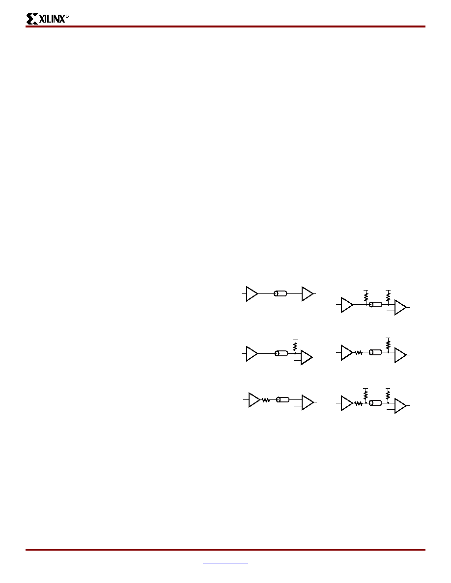
termination methods appears in Figure 41.
Simultaneous Switching Guidelines
Ground bounce can occur with high-speed digital ICs when
multiple outputs change states simultaneously, causing
undesired transient behavior on an output, or in the internal
logic. This problem is also referred to as the Simultaneous
Switching Output (SSO) problem.
Ground bounce is primarily due to current changes in the
combined inductance of ground pins, bond wires, and
Figure 41: Overview of Standard Input and Output
Termination Methods
DS001_41_032300
Unterminated
Double Parallel Terminated
Series-Parallel Terminated Output
Driving a Parallel Terminated Input
Series Terminated Output Driving
a Parallel Terminated Input
Unterminated Output Driving
a Parallel Terminated Input
V
TT
V
REF
V
REF
V
REF
V
REF
V
TT
V
TT
V
TT
V
TT
V
TT
Series Terminated Output
V
REF
Z=50
相关PDF资料 |
PDF描述 |
|---|---|
| 24LC22AT-I/SN | IC EEPROM 2KBIT 400KHZ 8SOIC |
| XC3S400A-4FT256C | IC SPARTAN-3A FPGA 400K 256FTBGA |
| XC3S200A-4FG320C | IC SPARTAN-3A FPGA 200K 320FBGA |
| XC2S50E-6PQ208C | IC FPGA 1.8V 384 CLB'S 208-PQFP |
| XC3S200A-4FT256I | IC SPARTAN-3A FPGA 200K 256FTBGA |
相关代理商/技术参数 |
参数描述 |
|---|---|
| XC2S100-5TQ144I | 功能描述:IC FPGA 2.5V I-TEMP 144-TQFP RoHS:否 类别:集成电路 (IC) >> 嵌入式 - FPGA(现场可编程门阵列) 系列:Spartan®-II 标准包装:40 系列:Spartan® 6 LX LAB/CLB数:3411 逻辑元件/单元数:43661 RAM 位总计:2138112 输入/输出数:358 门数:- 电源电压:1.14 V ~ 1.26 V 安装类型:表面贴装 工作温度:-40°C ~ 100°C 封装/外壳:676-BGA 供应商设备封装:676-FBGA(27x27) |
| XC2S100-5TQG144C | 功能描述:IC SPARTAN-II FPGA 100K 144-TQFP RoHS:是 类别:集成电路 (IC) >> 嵌入式 - FPGA(现场可编程门阵列) 系列:Spartan®-II 标准包装:60 系列:XP LAB/CLB数:- 逻辑元件/单元数:10000 RAM 位总计:221184 输入/输出数:244 门数:- 电源电压:1.71 V ~ 3.465 V 安装类型:表面贴装 工作温度:0°C ~ 85°C 封装/外壳:388-BBGA 供应商设备封装:388-FPBGA(23x23) 其它名称:220-1241 |
| XC2S100-5TQG144I | 制造商:Xilinx 功能描述:FPGA SPARTAN-II 100K GATES 2700 CELLS 263MHZ 2.5V 144TQFP EP - Trays 制造商:Xilinx 功能描述:XLXXC2S100-5TQG144I IC SYSTEM GATE |
| XC2S100-5VQ100C | 制造商:XILINX 制造商全称:XILINX 功能描述:Spartan-II 2.5V FPGA Family:Introduction and Ordering Information |
| XC2S100-5VQ100I | 制造商:XILINX 制造商全称:XILINX 功能描述:Spartan-II 2.5V FPGA Family:Introduction and Ordering Information |
发布紧急采购,3分钟左右您将得到回复。