参数资料
| 型号: | XC2S100-5TQ144C |
| 厂商: | Xilinx Inc |
| 文件页数: | 25/99页 |
| 文件大小: | 0K |
| 描述: | IC FPGA 2.5V 600 CLB'S 144-TQFP |
| 标准包装: | 60 |
| 系列: | Spartan®-II |
| LAB/CLB数: | 600 |
| 逻辑元件/单元数: | 2700 |
| RAM 位总计: | 40960 |
| 输入/输出数: | 92 |
| 门数: | 100000 |
| 电源电压: | 2.375 V ~ 2.625 V |
| 安装类型: | 表面贴装 |
| 工作温度: | 0°C ~ 85°C |
| 封装/外壳: | 144-LQFP |
| 供应商设备封装: | 144-TQFP(20x20) |
| 其它名称: | 122-1229 XC2S100-5TQ144C-ND |
第1页第2页第3页第4页第5页第6页第7页第8页第9页第10页第11页第12页第13页第14页第15页第16页第17页第18页第19页第20页第21页第22页第23页第24页当前第25页第26页第27页第28页第29页第30页第31页第32页第33页第34页第35页第36页第37页第38页第39页第40页第41页第42页第43页第44页第45页第46页第47页第48页第49页第50页第51页第52页第53页第54页第55页第56页第57页第58页第59页第60页第61页第62页第63页第64页第65页第66页第67页第68页第69页第70页第71页第72页第73页第74页第75页第76页第77页第78页第79页第80页第81页第82页第83页第84页第85页第86页第87页第88页第89页第90页第91页第92页第93页第94页第95页第96页第97页第98页第99页
Spartan-II FPGA Family: Functional Description
DS001-2 (v2.8) June 13, 2008
Module 2 of 4
Product Specification
31
R
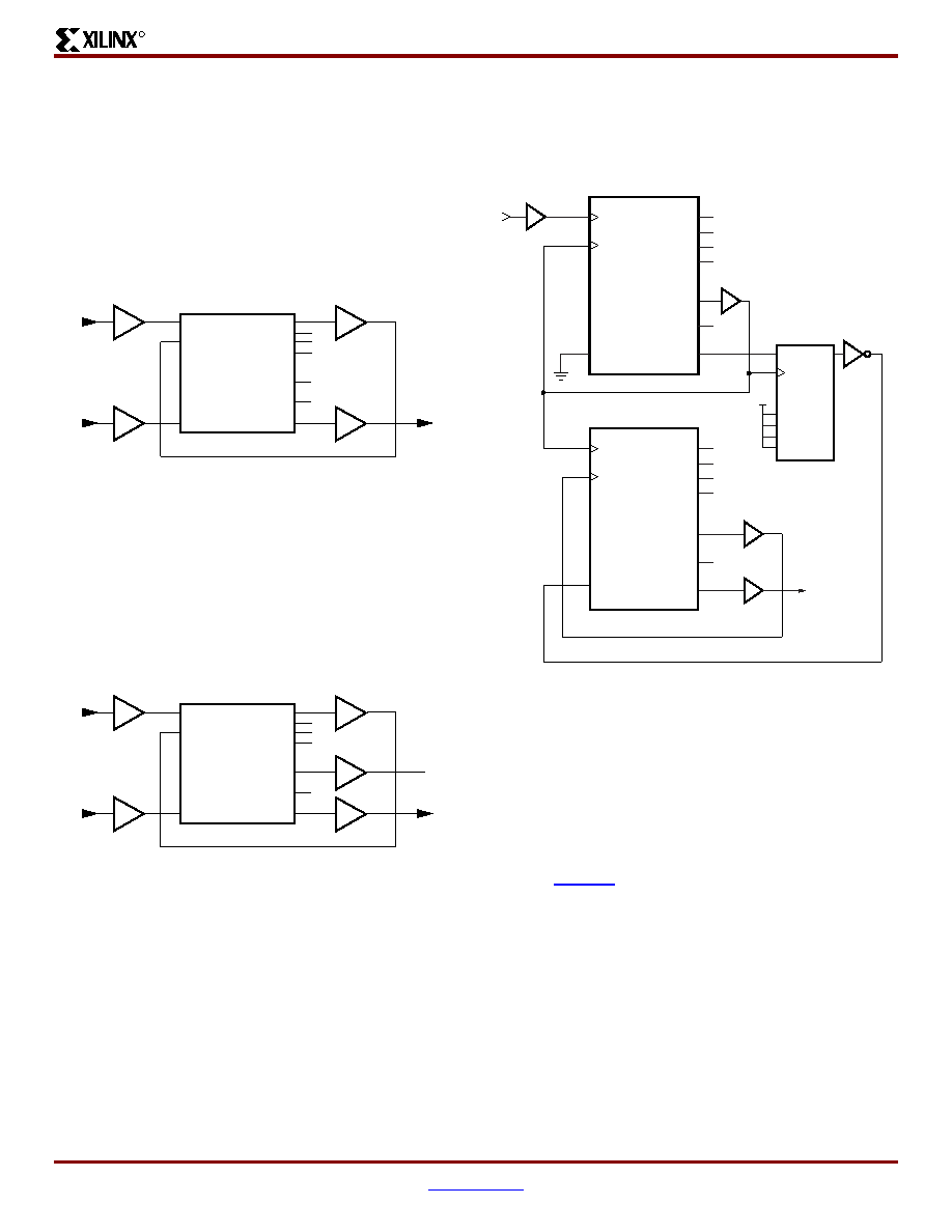
Useful Application Examples
The Spartan-II FPGA DLL can be used in a variety of
creative and useful applications. The following examples
show some of the more common applications.
Standard Usage
The circuit shown in Figure 28 resembles the BUFGDLL
macro implemented to provide access to the RST and
LOCKED pins of the CLKDLL.
Deskew of Clock and Its 2x Multiple
The circuit shown in Figure 29 implements a 2x clock
multiplier and also uses the CLK0 clock output with zero ns
skew between registers on the same chip. A clock divider
circuit could alternatively be implemented using similar
connections.
Because any single DLL can only access at most two
BUFGs, any additional output clock signals must be routed
from the DLL in this example on the high speed backbone
routing.
Generating a 4x Clock
By connecting two DLL circuits each implementing a 2x
clock multiplier in series as shown in Figure 30, a 4x clock
multiply can be implemented with zero skew between
registers in the same device.
If other clock output is needed, the clock could access a
BUFG only if the DLLs are constrained to exist on opposite
edges (Top or Bottom) of the device.
When using this circuit it is vital to use the SRL16 cell to
reset the second DLL after the initial chip reset. If this is not
done, the second DLL may not recognize the change of
frequencies from when the input changes from a 1x (25/75)
waveform to a 2x (50/50) waveform. It is not recommended
to cascade more than two DLLs.
For design examples and more information on using the
DLL, see XAPP174, Using Delay-Locked Loops in Spartan-II
FPGAs.
Figure 28: Standard DLL Implementation
Figure 29: DLL Deskew of Clock and 2x Multiple
CLK0
CLK90
CLK180
CLK270
CLK2X
CLKDV
LOCKED
CLKIN
CLKFB
RST
DS001_28_061200
CLKDLL
BUFG
IBUFG
OBUF
IBUF
CLK0
CLK90
CLK180
CLK270
CLK2X
CLKDV
LOCKED
CLKIN
CLKFB
RST
DS001_29_061200
CLKDLL
BUFG
IBUFG
OBUF
BUFG
IBUF
Figure 30: DLL Generation of 4x Clock
DS001_30_061200
RST
CLKFB
CLKIN
CLKDLL
LOCKED
CLKDV
INV
BUFG
OBUF
SRL16
D
A3
A2
A1
A0
WCLK
BUFG
Q
IBUFG
CLK2X
CLK0
CLK90
CLK180
CLK270
RST
CLKFB
CLKIN
CLKDLL
LOCKED
CLKDV
CLK2X
CLK0
CLK90
CLK180
CLK270
相关PDF资料 |
PDF描述 |
|---|---|
| 24LC22AT-I/SN | IC EEPROM 2KBIT 400KHZ 8SOIC |
| XC3S400A-4FT256C | IC SPARTAN-3A FPGA 400K 256FTBGA |
| XC3S200A-4FG320C | IC SPARTAN-3A FPGA 200K 320FBGA |
| XC2S50E-6PQ208C | IC FPGA 1.8V 384 CLB'S 208-PQFP |
| XC3S200A-4FT256I | IC SPARTAN-3A FPGA 200K 256FTBGA |
相关代理商/技术参数 |
参数描述 |
|---|---|
| XC2S100-5TQ144I | 功能描述:IC FPGA 2.5V I-TEMP 144-TQFP RoHS:否 类别:集成电路 (IC) >> 嵌入式 - FPGA(现场可编程门阵列) 系列:Spartan®-II 标准包装:40 系列:Spartan® 6 LX LAB/CLB数:3411 逻辑元件/单元数:43661 RAM 位总计:2138112 输入/输出数:358 门数:- 电源电压:1.14 V ~ 1.26 V 安装类型:表面贴装 工作温度:-40°C ~ 100°C 封装/外壳:676-BGA 供应商设备封装:676-FBGA(27x27) |
| XC2S100-5TQG144C | 功能描述:IC SPARTAN-II FPGA 100K 144-TQFP RoHS:是 类别:集成电路 (IC) >> 嵌入式 - FPGA(现场可编程门阵列) 系列:Spartan®-II 标准包装:60 系列:XP LAB/CLB数:- 逻辑元件/单元数:10000 RAM 位总计:221184 输入/输出数:244 门数:- 电源电压:1.71 V ~ 3.465 V 安装类型:表面贴装 工作温度:0°C ~ 85°C 封装/外壳:388-BBGA 供应商设备封装:388-FPBGA(23x23) 其它名称:220-1241 |
| XC2S100-5TQG144I | 制造商:Xilinx 功能描述:FPGA SPARTAN-II 100K GATES 2700 CELLS 263MHZ 2.5V 144TQFP EP - Trays 制造商:Xilinx 功能描述:XLXXC2S100-5TQG144I IC SYSTEM GATE |
| XC2S100-5VQ100C | 制造商:XILINX 制造商全称:XILINX 功能描述:Spartan-II 2.5V FPGA Family:Introduction and Ordering Information |
| XC2S100-5VQ100I | 制造商:XILINX 制造商全称:XILINX 功能描述:Spartan-II 2.5V FPGA Family:Introduction and Ordering Information |
发布紧急采购,3分钟左右您将得到回复。