参数资料
| 型号: | XC3S400AN-4FG400I |
| 厂商: | Xilinx Inc |
| 文件页数: | 29/123页 |
| 文件大小: | 0K |
| 描述: | IC FPGA SPARTAN 3AN 400FBGA |
| 标准包装: | 60 |
| 系列: | Spartan®-3AN |
| LAB/CLB数: | 896 |
| 逻辑元件/单元数: | 8064 |
| RAM 位总计: | 368640 |
| 输入/输出数: | 311 |
| 门数: | 400000 |
| 电源电压: | 1.14 V ~ 1.26 V |
| 安装类型: | 表面贴装 |
| 工作温度: | -40°C ~ 100°C |
| 封装/外壳: | 400-BGA |
| 供应商设备封装: | 400-FBGA(21x21) |
第1页第2页第3页第4页第5页第6页第7页第8页第9页第10页第11页第12页第13页第14页第15页第16页第17页第18页第19页第20页第21页第22页第23页第24页第25页第26页第27页第28页当前第29页第30页第31页第32页第33页第34页第35页第36页第37页第38页第39页第40页第41页第42页第43页第44页第45页第46页第47页第48页第49页第50页第51页第52页第53页第54页第55页第56页第57页第58页第59页第60页第61页第62页第63页第64页第65页第66页第67页第68页第69页第70页第71页第72页第73页第74页第75页第76页第77页第78页第79页第80页第81页第82页第83页第84页第85页第86页第87页第88页第89页第90页第91页第92页第93页第94页第95页第96页第97页第98页第99页第100页第101页第102页第103页第104页第105页第106页第107页第108页第109页第110页第111页第112页第113页第114页第115页第116页第117页第118页第119页第120页第121页第122页第123页
Spartan-3AN FPGA Family: DC and Switching Characteristics
DS557 (v4.1) April 1, 2011
Product Specification
13
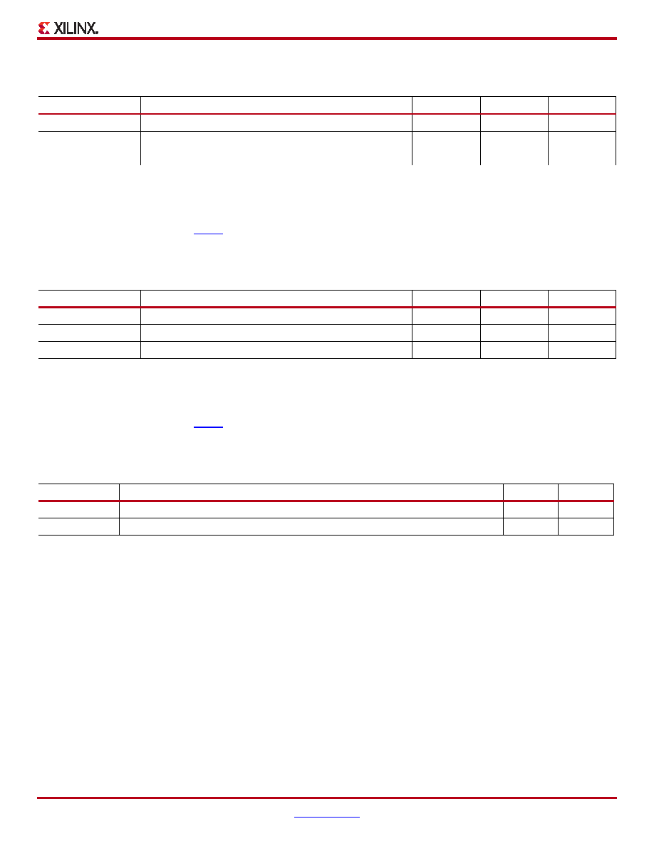
Power Supply Specifications
Table 7: Supply Voltage Thresholds for Power-On Reset
Symbol
Description
Min
Max
Units
VCCINTT
Threshold for the VCCINT supply
0.4
1.0
V
VCCAUXT
Threshold for the VCCAUX supply
1.0
2.0
V
VCCO2T
Threshold for the VCCO Bank 2 supply
1.0
2.0
V
Notes:
1.
When configuring from the In-System Flash, VCCAUX must be in the recommended operating range; on power-up make sure VCCAUX
reaches at least 3.0V before INIT_B goes High to indicate the start of configuration. VCCINT, VCCAUX, and VCCO supplies to the FPGA can
be applied in any order if this requirement is met. However, an external configuration source might have specific requirements. Check the
data sheet for the attached configuration source. Apply VCCINT last for lowest overall power consumption (see the chapter called “Powering
Spartan-3 Generation FPGAs” in UG331 for more information).
2.
To ensure successful power-on, VCCINT, VCCO Bank 2, and VCCAUX supplies must rise through their respective threshold-voltage ranges with
no dips at any point.
Table 8: Supply Voltage Ramp Rate
Symbol
Description
Min
Max
Units
VCCINTR
Ramp rate from GND to valid VCCINT supply level
0.2
100
ms
VCCAUXR
Ramp rate from GND to valid VCCAUX supply level
0.2
100
ms
VCCO2R
Ramp rate from GND to valid VCCO Bank 2 supply level
0.2
100
ms
Notes:
1.
When configuring from the In-System Flash, VCCAUX must be in the recommended operating range; on power-up make sure VCCAUX
reaches at least 3.0V before INIT_B goes High to indicate the start of configuration. VCCINT, VCCAUX, and VCCO supplies to the FPGA can
be applied in any order if this requirement is met. However, an external configuration source might have specific requirements. Check the
data sheet for the attached configuration source. Apply VCCINT last for lowest overall power consumption (see the chapter called “Powering
Spartan-3 Generation FPGAs” in UG331 for more information).
2.
To ensure successful power-on, VCCINT, VCCO Bank 2, and VCCAUX supplies must rise through their respective threshold-voltage ranges with
no dips at any point.
Table 9: Supply Voltage Levels Necessary for Preserving CMOS Configuration Latch (CCL) Contents and RAM Data
Symbol
Description
Min
Units
VDRINT
VCCINT level required to retain CMOS Configuration Latch (CCL) and RAM data
1.0
V
VDRAUX
VCCAUX level required to retain CMOS Configuration Latch (CCL) and RAM data
2.0
V
相关PDF资料 |
PDF描述 |
|---|---|
| XC3SD1800A-4CSG484LI | IC FPGA SPARTAN 3 DSP 484CSGBGA |
| XC3SD3400A-4FGG676I | SPARTAN-3ADSP FPGA 3400K 676FBGA |
| XC4036XLA-09HQ240C | IC FPGA C 2.5V 288 I/O 240HQFP |
| XC4062XL-09HQ240C | IC FPGA C-TEMP 3.3V 240-HQFP |
| XC4085XL-3BG560I | IC FPGA I-TEMP 3.3V 3SPD 560MBGA |
相关代理商/技术参数 |
参数描述 |
|---|---|
| XC3S400AN-4FG400I4100 | 制造商:Xilinx 功能描述: |
| XC3S400AN-4FGG400C | 功能描述:IC SPARTAN-3AN FPGA 400K 400FBGA RoHS:是 类别:集成电路 (IC) >> 嵌入式 - FPGA(现场可编程门阵列) 系列:Spartan®-3AN 标准包装:60 系列:XP LAB/CLB数:- 逻辑元件/单元数:10000 RAM 位总计:221184 输入/输出数:244 门数:- 电源电压:1.71 V ~ 3.465 V 安装类型:表面贴装 工作温度:0°C ~ 85°C 封装/外壳:388-BBGA 供应商设备封装:388-FPBGA(23x23) 其它名称:220-1241 |
| XC3S400AN-4FGG400CES | 制造商:Xilinx 功能描述: |
| XC3S400AN-4FGG400I | 功能描述:IC FPGA SPARTAN-3A 400K 400-FBGA RoHS:是 类别:集成电路 (IC) >> 嵌入式 - FPGA(现场可编程门阵列) 系列:Spartan®-3AN 标准包装:40 系列:Spartan® 6 LX LAB/CLB数:3411 逻辑元件/单元数:43661 RAM 位总计:2138112 输入/输出数:358 门数:- 电源电压:1.14 V ~ 1.26 V 安装类型:表面贴装 工作温度:-40°C ~ 100°C 封装/外壳:676-BGA 供应商设备封装:676-FBGA(27x27) |
| XC3S400AN-4FT256C | 制造商:Xilinx 功能描述:SPARTAN3AN - Trays 制造商:Xilinx 功能描述:IC FPGA SPARTAN-3AN 400K 256BGA 制造商:Xilinx 功能描述:IC FPGA 195 I/O 256FTBGA |
发布紧急采购,3分钟左右您将得到回复。