参数资料
| 型号: | XC3S50AN-4FTG256C |
| 厂商: | Xilinx Inc |
| 文件页数: | 72/123页 |
| 文件大小: | 0K |
| 描述: | IC FPGA SPARTAN-3AN 256FTBGA |
| 标准包装: | 90 |
| 系列: | Spartan®-3AN |
| LAB/CLB数: | 176 |
| 逻辑元件/单元数: | 1584 |
| RAM 位总计: | 55296 |
| 输入/输出数: | 195 |
| 门数: | 50000 |
| 电源电压: | 1.14 V ~ 1.26 V |
| 安装类型: | 表面贴装 |
| 工作温度: | 0°C ~ 85°C |
| 封装/外壳: | 256-LBGA |
| 供应商设备封装: | 256-FTBGA |
第1页第2页第3页第4页第5页第6页第7页第8页第9页第10页第11页第12页第13页第14页第15页第16页第17页第18页第19页第20页第21页第22页第23页第24页第25页第26页第27页第28页第29页第30页第31页第32页第33页第34页第35页第36页第37页第38页第39页第40页第41页第42页第43页第44页第45页第46页第47页第48页第49页第50页第51页第52页第53页第54页第55页第56页第57页第58页第59页第60页第61页第62页第63页第64页第65页第66页第67页第68页第69页第70页第71页当前第72页第73页第74页第75页第76页第77页第78页第79页第80页第81页第82页第83页第84页第85页第86页第87页第88页第89页第90页第91页第92页第93页第94页第95页第96页第97页第98页第99页第100页第101页第102页第103页第104页第105页第106页第107页第108页第109页第110页第111页第112页第113页第114页第115页第116页第117页第118页第119页第120页第121页第122页第123页
Spartan-3AN FPGA Family: DC and Switching Characteristics
DS557 (v4.1) April 1, 2011
Product Specification
52
Digital Clock Manager (DCM) Timing
For specification purposes, the DCM consists of three key
components: the Delay-Locked Loop (DLL), the Digital
Frequency Synthesizer (DFS), and the Phase Shifter (PS).
Aspects of DLL operation play a role in all DCM
applications. All such applications inevitably use the CLKIN
and the CLKFB inputs connected to either the CLK0 or the
CLK2X feedback, respectively. Thus, specifications in the
that only employs the DLL component. When the DFS
and/or the PS components are used together with the DLL,
then the specifications listed in the DFS and PS tables
ones in the DLL tables. DLL specifications that do not
change with the addition of DFS or PS functions are
Period jitter and cycle-cycle jitter are two of many different
ways of specifying clock jitter. Both specifications describe
statistical variation from a mean value.
Period jitter is the worst-case deviation from the ideal clock
period over a collection of millions of samples. In a
histogram of period jitter, the mean value is the clock period.
Cycle-cycle jitter is the worst-case difference in clock period
between adjacent clock cycles in the collection of clock
periods sampled. In a histogram of cycle-cycle jitter, the
mean value is zero.
Spread Spectrum
DCMs accept typical spread spectrum clocks as long as
they meet the input requirements. The DLL will track the
frequency changes created by the spread spectrum clock to
drive the global clocks to the FPGA logic. See XAPP469:
Spread-Spectrum Clocking Reception for Displays for
details.
Delay-Locked Loop (DLL)
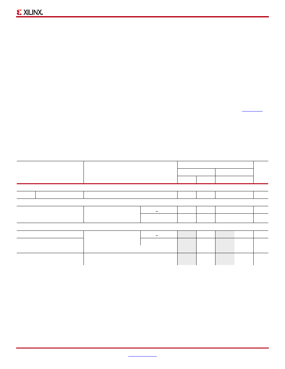
Table 39: Recommended Operating Conditions for the DLL
Symbol
Description
Speed Grade
Units
-5
-4
Min
Max
Min
Max
Input Frequency Ranges
FCLKIN
CLKIN_FREQ_DLL
Frequency of the CLKIN clock input
280(3)
250(3)
MHz
Input Pulse Requirements
CLKIN_PULSE
CLKIN pulse width as a
percentage of the CLKIN
period
FCLKIN < 150 MHz
40%
60%
40%
60%
%
FCLKIN > 150 MHz
45%
55%
45%
55%
%
Input Clock Jitter Tolerance and Delay Path Variation(4)
CLKIN_CYC_JITT_DLL_LF
Cycle-to-cycle jitter at the
CLKIN input
FCLKIN < 150 MHz
–±300
ps
CLKIN_CYC_JITT_DLL_HF
FCLKIN > 150 MHz
–±150
ps
CLKIN_PER_JITT_DLL
Period jitter at the CLKIN input
–±1
ns
CLKFB_DELAY_VAR_EXT
Allowable variation of off-chip feedback delay
from the DCM output to the CLKFB input
–±1
ns
Notes:
1.
DLL specifications apply when any of the DLL outputs (CLK0, CLK90, CLK180, CLK270, CLK2X, CLK2X180, or CLKDV) are in use.
2.
The DFS, when operating independently of the DLL, supports lower FCLKIN frequencies. See Table 41.
3.
The CLKIN_DIVIDE_BY_2 attribute can be used to increase the effective input frequency range up to FBUFG. When set to TRUE,
CLKIN_DIVIDE_BY_2 divides the incoming clock frequency by two as it enters the DCM.
4.
CLKIN input jitter beyond these limits might cause the DCM to lose lock.
5.
The DCM specifications are guaranteed when both adjacent DCMs are locked.
相关PDF资料 |
PDF描述 |
|---|---|
| XC3S50A-5FT256C | IC SPARTAN-3A FPGA 50K 256FTBGA |
| XC3S200-4VQG100C | SPARTAN-3A FPGA 200K STD 100VQFP |
| RSM44DSAS | CONN EDGECARD 88POS R/A .156 SLD |
| RMM44DSAS | CONN EDGECARD 88POS R/A .156 SLD |
| ASM12DRES | CONN EDGECARD 24POS .156 EYELET |
相关代理商/技术参数 |
参数描述 |
|---|---|
| XC3S50AN-4FTG256I | 功能描述:IC FPGA SPARTAN-3AN 256FTBGA RoHS:是 类别:集成电路 (IC) >> 嵌入式 - FPGA(现场可编程门阵列) 系列:Spartan®-3AN 标准包装:40 系列:Spartan® 6 LX LAB/CLB数:3411 逻辑元件/单元数:43661 RAM 位总计:2138112 输入/输出数:358 门数:- 电源电压:1.14 V ~ 1.26 V 安装类型:表面贴装 工作温度:-40°C ~ 100°C 封装/外壳:676-BGA 供应商设备封装:676-FBGA(27x27) |
| XC3S50AN-4TQ144I | 功能描述:IC FPGA SPARTAN 3AN 144TQFP RoHS:否 类别:集成电路 (IC) >> 嵌入式 - FPGA(现场可编程门阵列) 系列:Spartan®-3AN 标准包装:40 系列:Spartan® 6 LX LAB/CLB数:3411 逻辑元件/单元数:43661 RAM 位总计:2138112 输入/输出数:358 门数:- 电源电压:1.14 V ~ 1.26 V 安装类型:表面贴装 工作温度:-40°C ~ 100°C 封装/外壳:676-BGA 供应商设备封装:676-FBGA(27x27) |
| XC3S50AN-4TQG144C | 功能描述:IC SPARTAN-3AN FPGA 50K 144TQFP RoHS:是 类别:集成电路 (IC) >> 嵌入式 - FPGA(现场可编程门阵列) 系列:Spartan®-3AN 标准包装:60 系列:XP LAB/CLB数:- 逻辑元件/单元数:10000 RAM 位总计:221184 输入/输出数:244 门数:- 电源电压:1.71 V ~ 3.465 V 安装类型:表面贴装 工作温度:0°C ~ 85°C 封装/外壳:388-BBGA 供应商设备封装:388-FPBGA(23x23) 其它名称:220-1241 |
| XC3S50AN-4TQG144CES | 制造商:Xilinx 功能描述: |
| XC3S50AN-4TQG144I | 功能描述:IC FPGA SPARTAN-3AN50K 144-TQFP RoHS:是 类别:集成电路 (IC) >> 嵌入式 - FPGA(现场可编程门阵列) 系列:Spartan®-3AN 标准包装:60 系列:XP LAB/CLB数:- 逻辑元件/单元数:10000 RAM 位总计:221184 输入/输出数:244 门数:- 电源电压:1.71 V ~ 3.465 V 安装类型:表面贴装 工作温度:0°C ~ 85°C 封装/外壳:388-BBGA 供应商设备封装:388-FPBGA(23x23) 其它名称:220-1241 |
发布紧急采购,3分钟左右您将得到回复。