参数资料
| 型号: | XC3S50AN-4TQ144I |
| 厂商: | Xilinx Inc |
| 文件页数: | 75/123页 |
| 文件大小: | 0K |
| 描述: | IC FPGA SPARTAN 3AN 144TQFP |
| 标准包装: | 60 |
| 系列: | Spartan®-3AN |
| LAB/CLB数: | 176 |
| 逻辑元件/单元数: | 1584 |
| RAM 位总计: | 55296 |
| 输入/输出数: | 108 |
| 门数: | 50000 |
| 电源电压: | 1.14 V ~ 1.26 V |
| 安装类型: | 表面贴装 |
| 工作温度: | -40°C ~ 100°C |
| 封装/外壳: | 144-LQFP |
| 供应商设备封装: | 144-TQFP(20x20) |
第1页第2页第3页第4页第5页第6页第7页第8页第9页第10页第11页第12页第13页第14页第15页第16页第17页第18页第19页第20页第21页第22页第23页第24页第25页第26页第27页第28页第29页第30页第31页第32页第33页第34页第35页第36页第37页第38页第39页第40页第41页第42页第43页第44页第45页第46页第47页第48页第49页第50页第51页第52页第53页第54页第55页第56页第57页第58页第59页第60页第61页第62页第63页第64页第65页第66页第67页第68页第69页第70页第71页第72页第73页第74页当前第75页第76页第77页第78页第79页第80页第81页第82页第83页第84页第85页第86页第87页第88页第89页第90页第91页第92页第93页第94页第95页第96页第97页第98页第99页第100页第101页第102页第103页第104页第105页第106页第107页第108页第109页第110页第111页第112页第113页第114页第115页第116页第117页第118页第119页第120页第121页第122页第123页
Spartan-3AN FPGA Family: DC and Switching Characteristics
DS557 (v4.1) April 1, 2011
Product Specification
55
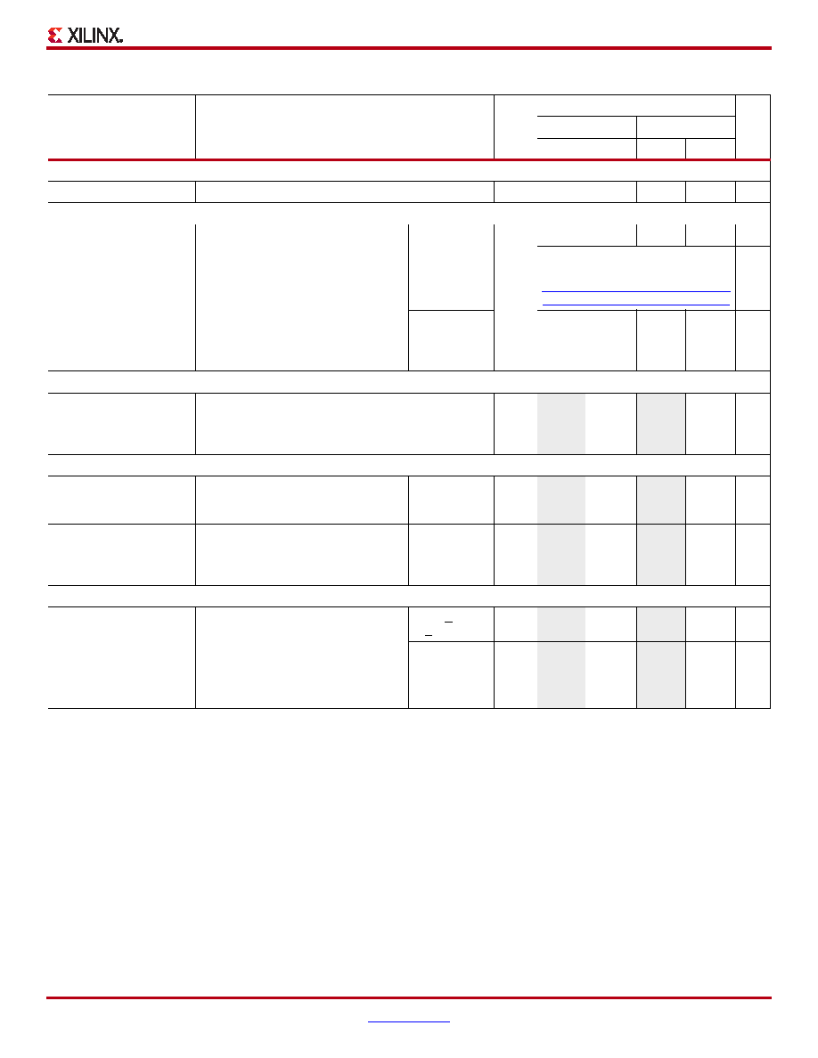
Table 42: Switching Characteristics for the DFS
Symbol
Description
Device
Speed Grade
Units
-5
-4
Min
Max
Min
Max
Output Frequency Ranges
CLKOUT_FREQ_FX
Frequency for the CLKFX and CLKFX180 outputs
All
5
350
5
320
MHz
Output Clock Jitter (2)(3)
CLKOUT_PER_JITT_FX
Period jitter at the CLKFX and
CLKFX180 outputs.
CLKIN
20 MHz
All
Typ
Max
Typ
Max
Use the Spartan-3A Jitter
Calculator:
ps
CLKIN
> 20 MHz
±[1% of
CLKFX
period
+ 100]
±[1% of
CLKFX
period
+ 200]
±[1% of
CLKFX
period
+ 100]
±[1% of
CLKFX
period
+ 200]
ps
Duty Cycle(4)(5)
CLKOUT_DUTY_CYCLE_FX
Duty cycle precision for the CLKFX and CLKFX180
outputs, including the BUFGMUX and clock tree
duty-cycle distortion
All
–±[1% of
CLKFX
period
+ 350]
–±[1% of
CLKFX
period
+ 350]
ps
Phase Alignment(5)
CLKOUT_PHASE_FX
Phase offset between the DFS CLKFX
output and the DLL CLK0 output when
both the DFS and DLL are used
All
–±200
ps
CLKOUT_PHASE_FX180 Phase offset between the DFS
CLKFX180 output and the DLL CLK0
output when both the DFS and DLL
are used
All
–±[1% of
CLKFX
period
+ 200]
–±[1% of
CLKFX
period
+ 200]
ps
Lock Time
LOCK_FX(2)
The time from deassertion at the
DCM’s Reset input to the rising
transition at its LOCKED output. The
DFS asserts LOCKED when the
CLKFX and CLKFX180 signals are
valid. If using both the DLL and the
DFS, use the longer locking time.
5 MHz < FCLKIN
< 15 MHz
All
–5
ms
FCLKIN >
15 MHz
–450
–
450
s
Notes:
1.
2.
For optimal jitter tolerance and faster lock time, use the CLKIN_PERIOD attribute.
3.
Maximum output jitter is characterized within a reasonable noise environment (40 SSOs and 25% CLB switching) on an XC3S1400A FPGA.
Output jitter strongly depends on the environment, including the number of SSOs, the output drive strength, CLB utilization, CLB switching
activities, switching frequency, power supply and PCB design. The actual maximum output jitter depends on the system application.
4.
The CLKFX and CLKFX180 outputs always have an approximate 50% duty cycle.
5.
Some duty-cycle and alignment specifications include a percentage of the CLKFX output period. For example, the data sheet specifies a
maximum CLKFX jitter of “±[1% of CLKFX period + 200]”. Assume the CLKFX output frequency is 100 MHz. The equivalent CLKFX period
is 10 ns and 1% of 10 ns is 0.1 ns or 100 ps. According to the data sheet, the maximum jitter is ±[100 ps + 200 ps] = ±300 ps.
相关PDF资料 |
PDF描述 |
|---|---|
| 748333-2 | CONTACT, HD22 PIN, 30AU |
| 748333-5 | CONTACT, HD22 PIN, FLAU |
| 24LC024-E/MS | IC EEPROM 2KBIT 400KHZ 8MSOP |
| 24C02CT-E/MNY | IC SRL EEPROM 256KX8 V 8-TDFN |
| 24LC08BT-E/MNY | IC EEPROM 8KBIT 400KHZ 8TDFN |
相关代理商/技术参数 |
参数描述 |
|---|---|
| XC3S50AN-4TQG144C | 功能描述:IC SPARTAN-3AN FPGA 50K 144TQFP RoHS:是 类别:集成电路 (IC) >> 嵌入式 - FPGA(现场可编程门阵列) 系列:Spartan®-3AN 标准包装:60 系列:XP LAB/CLB数:- 逻辑元件/单元数:10000 RAM 位总计:221184 输入/输出数:244 门数:- 电源电压:1.71 V ~ 3.465 V 安装类型:表面贴装 工作温度:0°C ~ 85°C 封装/外壳:388-BBGA 供应商设备封装:388-FPBGA(23x23) 其它名称:220-1241 |
| XC3S50AN-4TQG144CES | 制造商:Xilinx 功能描述: |
| XC3S50AN-4TQG144I | 功能描述:IC FPGA SPARTAN-3AN50K 144-TQFP RoHS:是 类别:集成电路 (IC) >> 嵌入式 - FPGA(现场可编程门阵列) 系列:Spartan®-3AN 标准包装:60 系列:XP LAB/CLB数:- 逻辑元件/单元数:10000 RAM 位总计:221184 输入/输出数:244 门数:- 电源电压:1.71 V ~ 3.465 V 安装类型:表面贴装 工作温度:0°C ~ 85°C 封装/外壳:388-BBGA 供应商设备封装:388-FPBGA(23x23) 其它名称:220-1241 |
| XC3S50AN-4TQG144ICES | 制造商:Xilinx 功能描述: |
| XC3S50AN-5FT256C | 制造商:Xilinx 功能描述:SPARTAN3AN - Trays 制造商:Xilinx 功能描述:IC FPGA SPARTAN-3AN 50K 256BGA 制造商:Xilinx 功能描述:IC FPGA 195 I/O 256FTBGA |
发布紧急采购,3分钟左右您将得到回复。