参数资料
| 型号: | XCS40-3PQ208I |
| 厂商: | Xilinx Inc |
| 文件页数: | 28/83页 |
| 文件大小: | 0K |
| 描述: | IC FPGA 5V I-TEMP 208-PQFP |
| 产品变化通告: | Spartan,Virtex FPGA/SCD Discontinuation 18/Oct/2010 |
| 标准包装: | 24 |
| 系列: | Spartan® |
| LAB/CLB数: | 784 |
| 逻辑元件/单元数: | 1862 |
| RAM 位总计: | 25088 |
| 输入/输出数: | 169 |
| 门数: | 40000 |
| 电源电压: | 4.5 V ~ 5.5 V |
| 安装类型: | 表面贴装 |
| 工作温度: | -40°C ~ 100°C |
| 封装/外壳: | 208-BFQFP |
| 供应商设备封装: | 208-PQFP(28x28) |
第1页第2页第3页第4页第5页第6页第7页第8页第9页第10页第11页第12页第13页第14页第15页第16页第17页第18页第19页第20页第21页第22页第23页第24页第25页第26页第27页当前第28页第29页第30页第31页第32页第33页第34页第35页第36页第37页第38页第39页第40页第41页第42页第43页第44页第45页第46页第47页第48页第49页第50页第51页第52页第53页第54页第55页第56页第57页第58页第59页第60页第61页第62页第63页第64页第65页第66页第67页第68页第69页第70页第71页第72页第73页第74页第75页第76页第77页第78页第79页第80页第81页第82页第83页
Spartan and Spartan-XL FPGA Families Data Sheet
34
DS060 (v2.0) March 1, 2013
Product Specification
R
Product Obsolete/Under Obsolescence
Configuration Sequence
There are four major steps in the Spartan/XL FPGA
power-up configuration sequence.
Configuration Memory Clear
Initialization
Configuration
Start-up
The full process is illustrated in Figure 30.
Configuration Memory Clear
When power is first applied or is reapplied to an FPGA, an
internal circuit forces initialization of the configuration logic.
When VCC reaches an operational level, and the circuit
passes the write and read test of a sample pair of configu-
ration bits, a time delay is started. This time delay is nomi-
nally 16 ms. The delay is four times as long when in Master
Serial Mode to allow ample time for all slaves to reach a sta-
ble VCC. When all INIT pins are tied together, as recom-
mended, the longest delay takes precedence. Therefore,
devices with different time delays can easily be mixed and
matched in a daisy chain.
This delay is applied only on power-up. It is not applied
when reconfiguring an FPGA by pulsing the PROGRAM pin
Low. During this time delay, or as long as the PROGRAM
input is asserted, the configuration logic is held in a Config-
uration Memory Clear state. The configuration-memory
frames are consecutively initialized, using the internal oscil-
lator.
At the end of each complete pass through the frame
addressing, the power-on time-out delay circuitry and the
level of the PROGRAM pin are tested. If neither is asserted,
the logic initiates one additional clearing of the configuration
frames and then tests the INIT input.
Initialization
During initialization and configuration, user pins HDC, LDC,
INIT and DONE provide status outputs for the system inter-
face. The outputs LDC, INIT and DONE are held Low and
HDC is held High starting at the initial application of power.
The open drain INIT pin is released after the final initializa-
tion pass through the frame addresses. There is a deliber-
ate delay before a Master-mode device recognizes an
inactive INIT. Two internal clocks after the INIT pin is recog-
nized as High, the device samples the MODE pin to deter-
mine the configuration mode. The appropriate interface
lines become active and the configuration preamble and
data can be loaded.
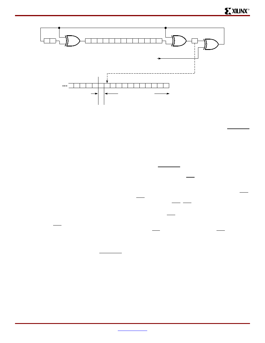
Figure 29: Circuit for Generating CRC-16
0
X2
2
3456789 10 11 12 13 14
1
X15
X16
15
SERIAL DATA IN
1
0 1514 13 12 1110 9
8
7
65
1
CRC – CHECKSUM
LAST DATA FRAME
START
BIT
DS060_29_080400
Polynomial: X16 + X15 + X2 + 1
Readback Data Stream
相关PDF资料 |
PDF描述 |
|---|---|
| XCS40-3PQ208C | IC FPGA 5V C-TEMP 208-PQFP |
| XCS40-3BG256C | IC FPGA 5V C-TEMP 256-PBGA |
| ASM15DRES | CONN EDGECARD 30POS .156 EYELET |
| FMC25DRYI-S93 | CONN EDGECARD 50POS .100 DIP SLD |
| ASC65DRTS-S93 | CONN EDGECARD 130PS DIP .100 SLD |
相关代理商/技术参数 |
参数描述 |
|---|---|
| XCS40-3PQ240C | 功能描述:IC FPGA 5V C-TEMP 240-PQFP RoHS:否 类别:集成电路 (IC) >> 嵌入式 - FPGA(现场可编程门阵列) 系列:Spartan® 标准包装:1 系列:Kintex-7 LAB/CLB数:25475 逻辑元件/单元数:326080 RAM 位总计:16404480 输入/输出数:350 门数:- 电源电压:0.97 V ~ 1.03 V 安装类型:表面贴装 工作温度:0°C ~ 85°C 封装/外壳:900-BBGA,FCBGA 供应商设备封装:900-FCBGA(31x31) 其它名称:122-1789 |
| XCS40-3PQ240I | 制造商:XILINX 制造商全称:XILINX 功能描述:Spartan and Spartan-XL Families Field Programmable Gate Arrays |
| XCS40-3PQ256C | 制造商:XILINX 制造商全称:XILINX 功能描述:Spartan and Spartan-XL Families Field Programmable Gate Arrays |
| XCS40-3PQ256I | 制造商:XILINX 制造商全称:XILINX 功能描述:Spartan and Spartan-XL Families Field Programmable Gate Arrays |
| XCS40-3PQ280C | 制造商:XILINX 制造商全称:XILINX 功能描述:Spartan and Spartan-XL Families Field Programmable Gate Arrays |
发布紧急采购,3分钟左右您将得到回复。