参数资料
| 型号: | XCS40-3PQ208I |
| 厂商: | Xilinx Inc |
| 文件页数: | 38/83页 |
| 文件大小: | 0K |
| 描述: | IC FPGA 5V I-TEMP 208-PQFP |
| 产品变化通告: | Spartan,Virtex FPGA/SCD Discontinuation 18/Oct/2010 |
| 标准包装: | 24 |
| 系列: | Spartan® |
| LAB/CLB数: | 784 |
| 逻辑元件/单元数: | 1862 |
| RAM 位总计: | 25088 |
| 输入/输出数: | 169 |
| 门数: | 40000 |
| 电源电压: | 4.5 V ~ 5.5 V |
| 安装类型: | 表面贴装 |
| 工作温度: | -40°C ~ 100°C |
| 封装/外壳: | 208-BFQFP |
| 供应商设备封装: | 208-PQFP(28x28) |
第1页第2页第3页第4页第5页第6页第7页第8页第9页第10页第11页第12页第13页第14页第15页第16页第17页第18页第19页第20页第21页第22页第23页第24页第25页第26页第27页第28页第29页第30页第31页第32页第33页第34页第35页第36页第37页当前第38页第39页第40页第41页第42页第43页第44页第45页第46页第47页第48页第49页第50页第51页第52页第53页第54页第55页第56页第57页第58页第59页第60页第61页第62页第63页第64页第65页第66页第67页第68页第69页第70页第71页第72页第73页第74页第75页第76页第77页第78页第79页第80页第81页第82页第83页
Spartan and Spartan-XL FPGA Families Data Sheet
DS060 (v2.0) March 1, 2013
43
Product Specification
R
Product Obsolete/Under Obsolescence
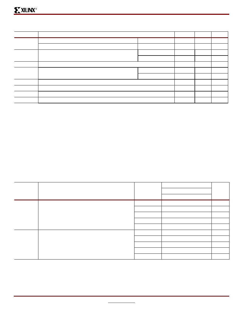
Spartan Family DC Characteristics Over Operating Conditions
Spartan Family Global Buffer Switching Characteristic Guidelines
All devices are 100% functionally tested. Internal timing
parameters are derived from measuring internal test pat-
terns. Listed below are representative values where one
global clock input drives one vertical clock line in each
accessible column, and where all accessible IOB and CLB
flip-flops are clocked by the global clock net.
When fewer vertical clock lines are connected, the clock dis-
tribution is faster; when multiple clock lines per column are
driven from the same global clock, the delay is longer. For
more specific, more precise, and worst-case guaranteed
data, reflecting the actual routing structure, use the values
provided by the static timing analyzer (TRCE in the Xilinx
Development System) and back-annotated to the simulation
netlist. These path delays, provided as a guideline, have
been extracted from the static timing analyzer report. All
timing parameters assume worst-case operating conditions
(supply voltage and junction temperature).
Symbol
Description
Min
Max
Units
VOH
High-level output voltage @ IOH = –4.0 mA, VCC min
TTL outputs
2.4
-
V
High-level output voltage @ IOH = –1.0 mA, VCC min
CMOS outputs
VCC – 0.5
-
V
VOL
Low-level output voltage @ IOL = 12.0 mA, VCC min(1)
TTL outputs
-
0.4
V
CMOS outputs
-
0.4
V
VDR
Data retention supply voltage (below which configuration data may be lost)
3.0
-
V
ICCO
Quiescent FPGA supply current(2)
Commercial
-
3.0
mA
Industrial
-
6.0
mA
IL
Input or output leakage current
–10
+10
μA
CIN
Input capacitance (sample tested)
-
10
pF
IRPU
Pad pull-up (when selected) @ VIN = 0V (sample tested)
0.02
0.25
mA
IRPD
Pad pull-down (when selected) @ VIN = 5V (sample tested)
0.02
-
mA
Notes:
1.
With 50% of the outputs simultaneously sinking 12 mA, up to a maximum of 64 pins.
2.
With no output current loads, no active input pull-up resistors, all package pins at VCC or GND, and the FPGA configured with a Tie
option.
Symbol
Description
Device
Speed Grade
Units
-4
-3
Max
TPG
From pad through Primary buffer, to any clock K
XCS05
2.0
4.0
ns
XCS10
2.4
4.3
ns
XCS20
2.8
5.4
ns
XCS30
3.2
5.8
ns
XCS40
3.5
6.4
ns
TSG
From pad through Secondary buffer, to any clock K
XCS05
2.5
4.4
ns
XCS10
2.9
4.7
ns
XCS20
3.3
5.8
ns
XCS30
3.6
6.2
ns
XCS40
3.9
6.7
ns
相关PDF资料 |
PDF描述 |
|---|---|
| XCS40-3PQ208C | IC FPGA 5V C-TEMP 208-PQFP |
| XCS40-3BG256C | IC FPGA 5V C-TEMP 256-PBGA |
| ASM15DRES | CONN EDGECARD 30POS .156 EYELET |
| FMC25DRYI-S93 | CONN EDGECARD 50POS .100 DIP SLD |
| ASC65DRTS-S93 | CONN EDGECARD 130PS DIP .100 SLD |
相关代理商/技术参数 |
参数描述 |
|---|---|
| XCS40-3PQ240C | 功能描述:IC FPGA 5V C-TEMP 240-PQFP RoHS:否 类别:集成电路 (IC) >> 嵌入式 - FPGA(现场可编程门阵列) 系列:Spartan® 标准包装:1 系列:Kintex-7 LAB/CLB数:25475 逻辑元件/单元数:326080 RAM 位总计:16404480 输入/输出数:350 门数:- 电源电压:0.97 V ~ 1.03 V 安装类型:表面贴装 工作温度:0°C ~ 85°C 封装/外壳:900-BBGA,FCBGA 供应商设备封装:900-FCBGA(31x31) 其它名称:122-1789 |
| XCS40-3PQ240I | 制造商:XILINX 制造商全称:XILINX 功能描述:Spartan and Spartan-XL Families Field Programmable Gate Arrays |
| XCS40-3PQ256C | 制造商:XILINX 制造商全称:XILINX 功能描述:Spartan and Spartan-XL Families Field Programmable Gate Arrays |
| XCS40-3PQ256I | 制造商:XILINX 制造商全称:XILINX 功能描述:Spartan and Spartan-XL Families Field Programmable Gate Arrays |
| XCS40-3PQ280C | 制造商:XILINX 制造商全称:XILINX 功能描述:Spartan and Spartan-XL Families Field Programmable Gate Arrays |
发布紧急采购,3分钟左右您将得到回复。