- 您现在的位置:买卖IC网 > PDF目录33761 > 42S16400A (Integrated Silicon Solution, Inc.) 1 Meg Bits x 16 Bits x 4 Banks (64-MBIT) SYNCHRONOUS DYNAMIC RAM PDF资料下载
参数资料
| 型号: | 42S16400A |
| 厂商: | Integrated Silicon Solution, Inc. |
| 英文描述: | 1 Meg Bits x 16 Bits x 4 Banks (64-MBIT) SYNCHRONOUS DYNAMIC RAM |
| 中文描述: | 1梅格位× 16位× 4银行(64兆位)同步动态RAM |
| 文件页数: | 13/55页 |
| 文件大小: | 472K |
| 代理商: | 42S16400A |
第1页第2页第3页第4页第5页第6页第7页第8页第9页第10页第11页第12页当前第13页第14页第15页第16页第17页第18页第19页第20页第21页第22页第23页第24页第25页第26页第27页第28页第29页第30页第31页第32页第33页第34页第35页第36页第37页第38页第39页第40页第41页第42页第43页第44页第45页第46页第47页第48页第49页第50页第51页第52页第53页第54页第55页
IS42S16400A
ISSI
20
Integrated Silicon Solution, Inc. — www.issi.com — 1-800-379-4774
Rev.C
04/16/03
CLK
CKE
HIGH-Z
COLUMN ADDRESS
AUTO PRECHARGE
NO PRECHARGE
CS
RAS
CAS
WE
A0-A7
A10
BA0, BA1
BANK ADDRESS
A8,A9,A11
READ COMMAND
READS
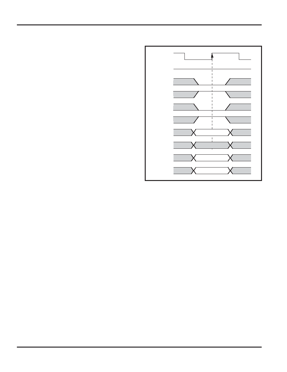
READ bursts are initiated with a READ command, as
shown in the READ COMMAND diagram.
The starting column and bank addresses are provided with
the READ command, and auto precharge is either enabled
or disabled for that burst access. If auto precharge is
enabled, the row being accessed is precharged at the
completion of the burst. For the generic READ commands
used in the following illustrations, auto precharge is disabled.
During READ bursts, the valid data-out element from the
starting column address will be available following the
CAS latency after the READ command. Each subsequent
data-out element will be valid by the next positive clock
edge. The CAS Latency diagram shows general timing
for each possible CAS latency setting.
Upon completion of a burst, assuming no other commands
have been initiated, the DQs will go High-Z. A full-page
burst will continue until terminated. (At the end of the page,
it will wrap to column 0 and continue.)
Data from any READ burst may be truncated with a
subsequent READ command, and data from a fixed-length
READ burst may be immediately followed by data from a
READ command. In either case, a continuous flow of data
can be maintained. The first data element from the new
burst follows either the last element of a completed burst or
the last desired data element of a longer burst which is
being truncated.
The new READ command should be issued
x cycles
before the clock edge at which the last desired data
element is valid, where
x equals the CAS latency minus
one. This is shown in Consecutive READ Bursts for CAS
latencies of two and three; data element
n + 3 is either the
last of a burst of four or the last desired of a longer burst.
The 64Mb SDRAM uses a pipelined architecture and
therefore does not require the
2n rule associated with a
prefetch architecture. A READ command can be initiated
on any clock cycle following a previous READ command.
Full-speed random read accesses can be performed to the
same bank, as shown in Random READ Accesses, or each
subsequent READ may be performed to a different bank.
Data from any READ burst may be truncated with a
subsequent WRITE command, and data from a fixed-length
READ burst may be immediately followed by data from a
WRITE command (subject to bus turnaround limitations).
The WRITE burst may be initiated on the clock edge
immediately following the last (or last desired) data
element from the READ burst, provided that I/O contention
can be avoided. In a given system design, there may be
a possibility that the device driving the input data will go
Low-Z before the SDRAM DQs go High-Z. In this case, at
least a single-cycle delay should occur between the last
read data and the WRITE command.
The DQM input is used to avoid I/O contention, as shown
in Figures RW1 and RW2. The DQM signal must be
asserted (HIGH) at least two clocks prior to the WRITE
command (DQM latency is two clocks for output buffers)
to suppress data-out from the READ. Once the WRITE
command is registered, the DQs will go High-Z (or remain
High-Z), regardless of the state of the DQM signal,
provided the DQM was active on the clock just prior to the
WRITE command that truncated the READ command. If
not, the second WRITE will be an invalid WRITE. For
example, if DQM was LOW during T4 in Figure RW2, then
the WRITEs at T5 and T7 would be valid, while the WRITE
at T6 would be invalid.
The DQM signal must be de-asserted prior to the WRITE
command (DQM latency is zero clocks for input buffers)
to ensure that the written data is not masked. Figure RW1
shows the case where the clock frequency allows for bus
contention to be avoided without adding a NOP cycle, and
Figure RW2 shows the case where the additional NOP is
needed.
A fixed-length READ burst may be followed by, or truncated
with, a PRECHARGE command to the same bank (provided
that auto precharge was not activated), and a full-page burst
may be truncated with a PRECHARGE command to the
相关PDF资料 |
PDF描述 |
|---|---|
| 42S16800A | 16Meg x 8, 8Meg x16 & 4Meg x 32 128-MBIT SYNCHRONOUS DRAM |
| 42S32200 | 512K Bits x 32 Bits x 4 Banks (64-MBIT) SYNCHRONOUS DYNAMIC RAM |
| 4300-000 | EMI/RFI FILTER Hermetically Sealed |
| 4300-000LF | |
| 4300-001 | EMI/RFI FILTER Hermetically Sealed |
相关代理商/技术参数 |
参数描述 |
|---|---|
| 42S16400B-6TLTR | 制造商:Integrated Silicon Solution Inc 功能描述: |
| 42S16800A | 制造商:ISSI 制造商全称:Integrated Silicon Solution, Inc 功能描述:16Meg x 8, 8Meg x16 & 4Meg x 32 128-MBIT SYNCHRONOUS DRAM |
| 42S16800L | 制造商:NEC 制造商全称:NEC 功能描述:3.3 V OPERATION 16 M-BIT DYNAMIC RAM 2 M-WORD BY 8-BIT, FAST PAGE MODE |
| 42S16800L-A60 | 制造商:NEC 制造商全称:NEC 功能描述:3.3 V OPERATION 16 M-BIT DYNAMIC RAM 2 M-WORD BY 8-BIT, FAST PAGE MODE |
| 42S16800L-A70 | 制造商:NEC 制造商全称:NEC 功能描述:3.3 V OPERATION 16 M-BIT DYNAMIC RAM 2 M-WORD BY 8-BIT, FAST PAGE MODE |
发布紧急采购,3分钟左右您将得到回复。