- 您现在的位置:买卖IC网 > PDF目录378244 > 85C30 (Advanced Micro Devices, Inc.) Enhanced Serial Communications Controller PDF资料下载
参数资料
| 型号: | 85C30 |
| 厂商: | Advanced Micro Devices, Inc. |
| 英文描述: | Enhanced Serial Communications Controller |
| 中文描述: | 增强的串行通信控制器 |
| 文件页数: | 27/68页 |
| 文件大小: | 528K |
| 代理商: | 85C30 |
第1页第2页第3页第4页第5页第6页第7页第8页第9页第10页第11页第12页第13页第14页第15页第16页第17页第18页第19页第20页第21页第22页第23页第24页第25页第26页当前第27页第28页第29页第30页第31页第32页第33页第34页第35页第36页第37页第38页第39页第40页第41页第42页第43页第44页第45页第46页第47页第48页第49页第50页第51页第52页第53页第54页第55页第56页第57页第58页第59页第60页第61页第62页第63页第64页第65页第66页第67页第68页
AMD
27
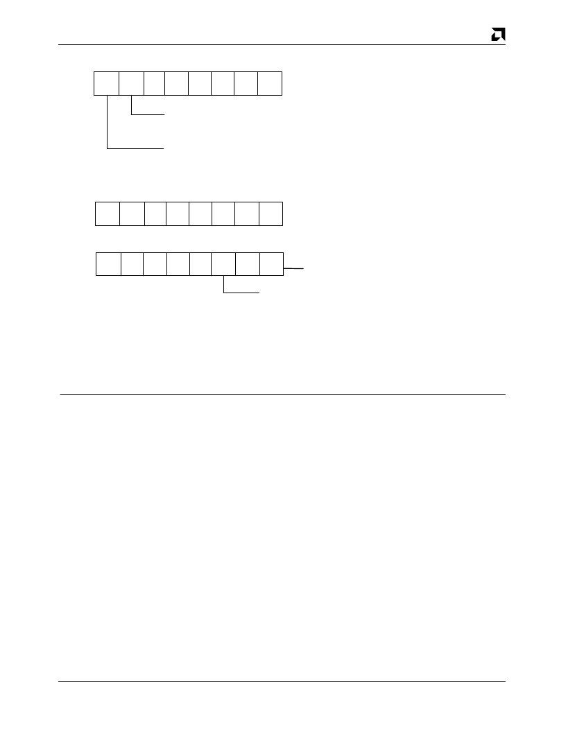
Am85C30
7
6
5
4
3
2
1
0
FOY FDA
BC
13
BC
12
BC
11
BC
10
BC
9
BC
8
RR7
FIFO Data Available Status
1 = Status Reads Will Come From FIFO
0 = Status Reads Will Come From SCC
FIFO Overflow Status
1 = FIFO Overflowed During Operation
0 = Normal
BC
7
BC
BC
BC
BC
BC
BC
BC
RR6
Read From FIFO
LSB Byte Count
RR15
ENH
FEN
Status FIFO Enable Control Bit
1 = Status and Byte Count Will be
Held in the Status FIFO Until Read
0 = Status Will Not be Held (SCC Emulation Mode)
= No Change From NMOS SCC DFN
6
5
4
3
2
1
0
7
6
5
4
3
2
1
0
7
6
5
4
3
2
1
0
ENH: SDLC/HDLC Enhancement Status
1 = Enhancements Enabled
0 = Enhancements Disabled
Figure 15. SCC Additional Registers
10216F-19
Enable
The byte counter is enabled when the SCC is in the
SDLC/HDLC mode and WR15 bit 2 is set to 1.
Reset
The byte counter is reset whenever an SDLC flag char-
acter is received. The reset is timed so that the contents
of the byte counter are successfully written into the
FIFO.
Increment
The byte counter is incremented by writes to the data
FIFO. The counter represents the number of bytes re-
ceived by the SCC, rather than the number of bytes
transferred from the SCC. (These counts may differ by
up to the number of bytes in the receive data FIFO con-
tained in the SCC.)
Am85C30 SDLC/HDLC Enhancement
Register Access
SDLC/HDLC enhancements on the Am85C30 are en-
abled or disabled via bits D
2
or D
0
in WR15. Bit D
2
deter-
mines whether or not the 10
×
19 bit SDLC/HDLC
frame status FIFO is enabled while bit D
0
determines
whether or not other enhancements are enabled via
WR7
′
. Table 3 shows what functions on the Am85C30
are enabled when these bits are set.
When bit D
2
of WR15 is set to 1, two additional registers
(RR6 and RR7) per channel specific to the 10
×
19 bit
Frame Status FIFO are made available. The Am85C30
register map when this function is enabled is shown in
Table 4.
Bit D
0
of WR15 determines whether or not other en-
hancements pertinent only to SDLC/HDLC mode opera-
tion are available for programming via WR7
′
as shown
below. Write Register 7 prime (WR7
′
) can be written to
when bit D
0
of WR15 is set to 1. When this bit is set, writ-
ing to WR7 (flag register) actually writes to WR7
′
. If bit
D
6
of this register is set to 1, previously unreadable reg-
isters WR3, WR4, WR5, and WR10 are readable by the
pro-cessor. In addition, WR7
′
is also readable by having
this bit set. WR3 is read when a bogus RR9 register is
accessed during a read cycle. WR10 is read by access-
ing RR11, and WR7
′
is accessed by executing a read to
RR14. The Am85C30 register map with bit D
0
of WR15
and bit D
6
of WR7
′
set is shown in Table 5.
If both bits D
0
and D
2
of WR15 are set to 1 and D
6
of
WR7
′
is set to 1, then the Am85C30 register map is as
shown in Table 6.
相关PDF资料 |
PDF描述 |
|---|---|
| 85C72 | 1K CMOS Serial EEPROM(1K位,5.0V CMOS串行EEPROM) |
| 85C82 | 2K CMOS Serial EEPROM(2K位,5.0V CMOS串行EEPROM) |
| 85C92 | 4K CMOS Serial EEPROM(4K位,5.0V CMOS串行EEPROM) |
| 85CNQ015APBF | SCHOTTKY RECTIFIER New GenIII D-61 Package |
| 85CNQ015ASMPBF | SCHOTTKY RECTIFIER New GenIII D-61 Package |
相关代理商/技术参数 |
参数描述 |
|---|---|
| 85C5122DVB-RDTUM | 功能描述:开发板和工具包 - 8051 RAM Indus Green RoHS:否 制造商:Silicon Labs 产品:Development Kits 工具用于评估:C8051F960, Si7005 核心: 接口类型:USB 工作电源电压: |
| 85C51SND3B1 | 制造商:ATMEL 制造商全称:ATMEL Corporation 功能描述:Single-Chip Digital Audio Decoder - Encoder with USB 2.0 Interface |
| 85C51SND3B1N-7FTUL | 制造商:ATMEL 制造商全称:ATMEL Corporation 功能描述:Single-Chip Digital Audio Decoder - Encoder with USB 2.0 Interface |
| 85C51SND3B1N-RTTUL | 制造商:ATMEL 制造商全称:ATMEL Corporation 功能描述:Single-Chip Digital Audio Decoder - Encoder with USB 2.0 Interface |
| 85C51SND3B1N-UL | 制造商:ATMEL 制造商全称:ATMEL Corporation 功能描述:Single-Chip Digital Audio Decoder - Encoder with USB 2.0 Interface |
发布紧急采购,3分钟左右您将得到回复。