- 您现在的位置:买卖IC网 > PDF目录10031 > AD6654CBCZ (Analog Devices Inc)IC ADC 14BIT W/4CH RSP 256CSPBGA PDF资料下载
参数资料
| 型号: | AD6654CBCZ |
| 厂商: | Analog Devices Inc |
| 文件页数: | 24/88页 |
| 文件大小: | 0K |
| 描述: | IC ADC 14BIT W/4CH RSP 256CSPBGA |
| 标准包装: | 1 |
| 位数: | 14 |
| 采样率(每秒): | 92.16M |
| 数据接口: | 串行,并联 |
| 转换器数目: | 1 |
| 功率耗散(最大): | 2.5W |
| 电压电源: | 模拟和数字 |
| 工作温度: | -25°C ~ 85°C |
| 安装类型: | 表面贴装 |
| 封装/外壳: | 256-BGA,CSPBGA |
| 供应商设备封装: | 256-CSPBGA(17x17) |
| 包装: | 托盘 |
| 输入数目和类型: | 1 个差分,单极 |
第1页第2页第3页第4页第5页第6页第7页第8页第9页第10页第11页第12页第13页第14页第15页第16页第17页第18页第19页第20页第21页第22页第23页当前第24页第25页第26页第27页第28页第29页第30页第31页第32页第33页第34页第35页第36页第37页第38页第39页第40页第41页第42页第43页第44页第45页第46页第47页第48页第49页第50页第51页第52页第53页第54页第55页第56页第57页第58页第59页第60页第61页第62页第63页第64页第65页第66页第67页第68页第69页第70页第71页第72页第73页第74页第75页第76页第77页第78页第79页第80页第81页第82页第83页第84页第85页第86页第87页第88页
AD6654
Rev. 0 | Page 30 of 88
input clock cycle, as long as the input signal remains below the
lower threshold register value. If the counter reaches 1, the gain
control output is incremented by 1. If the signal goes above the
lower threshold register value, the gain adjustment is not made,
and the normal comparison to lower and upper threshold
registers is initiated once again. Therefore, the dwell timer
provides temporal hysteresis and prevents the gain from
continuously switching.
In a typical application, if the ADC signal goes below the lower
threshold for a time greater than the dwell time, then the gain
control output is incremented by 1. Gain control bits control the
gain ranging block, which appears before the ADC in the signal
chain. With each increment of the gain control output, gain in
the gain-ranging block is increased by 6.02 dB. This increases
the dynamic range of the input signal into the ADC by 6.02 dB.
This gain is compensated for in the AD6654 by relinearizing, as
explained in the Relinearization section. Therefore, the AD6654
can increase the dynamic range of the ADC by 42 dB, provided
that the gain-ranging block can support it.
Relinearization
The gain in the gain-ranging block (external) is compensated
for by relinearizing, using the exponent bits EXP[2:0] of the
input port. For this purpose, the gain control bits are connected
to the EXP[2:0] bits, providing an attenuation of 6.02 dB for
every increase in the gain control output. After the gain in the
external gain-ranging block and the attenuation in the AD6654
(using EXP bits), the signal gain is essentially unchanged. The
only change is the increase in the dynamic range of the ADC.
External gain-ranging blocks have a delay associated with
changing the gain of the signal. Typically, these delays can be
up to 14 clock cycles. The gain change in the AD6654 (via
EXP[2:0]) must be synchronized with the gain change in the
gain-ranging block (external). This is allowed in the AD6654 by
providing a flexible delay, programmable 6-bit word in the gain
control register. The value in this 6-bit word gives the delay in
input clock cycles. A programmable pipeline delay given by the
6-bit value (maximum delay of 63 clock cycles) is placed
between the gain control output and the EXP[2:0] input.
Therefore, the external gain-ranging block’s settling delays
are compensated for in the AD6654.
Note that any gain changes that are initiated during the relinear-
ization period are ignored. For example, if the AD6654 detects
that a gain adjustment is required during the relinearization
period of a previous gain adjustment, then the new adjustment
is ignored.
Setting Up the Gain Control Block
To set up the gain control block for the input port, the individ-
ual upper threshold registers and lower threshold registers
should be written with appropriate values. The 10-bit values
written into upper and lower threshold registers are compared
to the 10 MSBs of the absolute magnitude calculated using the
input port data. The 20-bit dwell-time register should have the
appropriate number of clock cycles to provide temporal
hysteresis.
A 6-bit relinearization pipeline delay word is set to synchronize
with the settling delay in the external gain-ranging circuitry.
Finally, the gain control enable bit is written with Logic 1 to
activate the gain control block. On enabling, the gain control
output bits are made 000 (output on EXP[2:0] pins), which
represent the minimum gain for the external gain-ranging
circuitry and corresponding minimum attenuation during
relinearization. The normal functioning takes over, as explained
previously in this section.
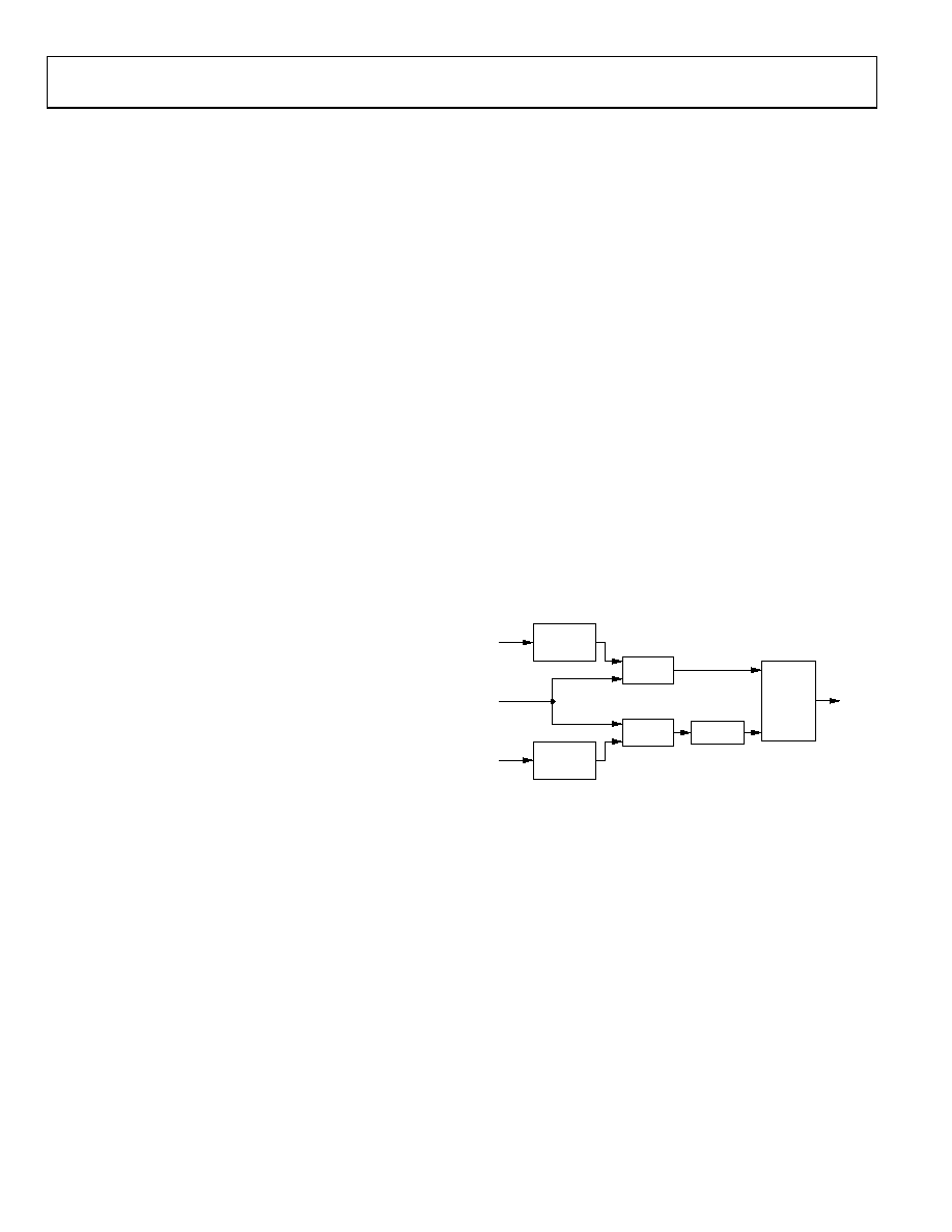
05156-032
DWELL
TIMER
COMPARE
A
< B
DEC
INC
EXP GEN
FROM
MEMORY
MAP
EXP [2:0]
A
B
LOWER
THRESHOLD
REGISTER
COMPARE
A
> B
FROM
MEMORY
MAP
B
A
UPPER
THRESHOLD
REGISTER
FROM INPUT
PORTS
INCREASE
EXTERNAL GAIN
DECREASE
EXTERNAL GAIN
Figure 43. Gain Control Block Diagram
相关PDF资料 |
PDF描述 |
|---|---|
| MS27467T21A16PA | CONN PLUG 16POS STRAIGHT W/PINS |
| VE-21J-IU-F1 | CONVERTER MOD DC/DC 36V 200W |
| MS3100R28-21S | CONN RCPT 37POS WALL MNT W/SCKT |
| VI-26H-MX-F4 | CONVERTER MOD DC/DC 52V 75W |
| VE-21H-IU-F3 | CONVERTER MOD DC/DC 52V 200W |
相关代理商/技术参数 |
参数描述 |
|---|---|
| AD6654XBCZ | 制造商:Analog Devices 功能描述:14-BIT, 92.16 MSPS, 4 & 6-CHANNEL WIDEBAND IF TO BASE BAND R - Bulk |
| AD6655 | 制造商:AD 制造商全称:Analog Devices 功能描述:IF Diversity Receiver |
| AD6655-125EBZ | 功能描述:BOARD EVAL W/AD6655 & SOFTWARE RoHS:是 类别:RF/IF 和 RFID >> RF 评估和开发套件,板 系列:- 标准包装:1 系列:- 类型:GPS 接收器 频率:1575MHz 适用于相关产品:- 已供物品:模块 其它名称:SER3796 |
| AD6655-125EBZ1 | 制造商:AD 制造商全称:Analog Devices 功能描述:IF Diversity Receiver |
| AD6655-150EBZ | 功能描述:BOARD EVAL FOR 150MSPS AD6655 RoHS:是 类别:RF/IF 和 RFID >> RF 评估和开发套件,板 系列:- 标准包装:1 系列:- 类型:GPS 接收器 频率:1575MHz 适用于相关产品:- 已供物品:模块 其它名称:SER3796 |
发布紧急采购,3分钟左右您将得到回复。