- 您现在的位置:买卖IC网 > PDF目录10149 > AD7712ARZ-REEL (Analog Devices Inc)IC ADC 24BIT SGNL CONDTNR 24SOIC PDF资料下载
参数资料
| 型号: | AD7712ARZ-REEL |
| 厂商: | Analog Devices Inc |
| 文件页数: | 11/28页 |
| 文件大小: | 0K |
| 描述: | IC ADC 24BIT SGNL CONDTNR 24SOIC |
| 标准包装: | 1,000 |
| 位数: | 24 |
| 采样率(每秒): | 1.03k |
| 数据接口: | 串行 |
| 转换器数目: | 1 |
| 功率耗散(最大): | 45mW |
| 电压电源: | 模拟和数字,双 ± |
| 工作温度: | -40°C ~ 85°C |
| 安装类型: | 表面贴装 |
| 封装/外壳: | 24-SOIC(0.295",7.50mm 宽) |
| 供应商设备封装: | 24-SOIC W |
| 包装: | 带卷 (TR) |
| 输入数目和类型: | 1 个单端,单极;1 个差分,单极;1 个差分,双极 |
第1页第2页第3页第4页第5页第6页第7页第8页第9页第10页当前第11页第12页第13页第14页第15页第16页第17页第18页第19页第20页第21页第22页第23页第24页第25页第26页第27页第28页
REV. F
AD7712
–19–
Table VI. Calibration Truth Table
Cal Type
MD2, MD1, MD0
Zero-Scale Cal
Full-Scale Cal
Sequence
Duration
Self-Cal
0, 0, 1
Shorted Inputs
VREF
One-Step
9
1/Output Rate
System Cal
0, 1, 0
AIN
–
Two-Step
4
1/Output Rate
System Cal
0, 1, 1
–
AIN
Two-Step
4
1/Output Rate
System Offset Cal
1, 0, 0
AIN
VREF
One-Step
9
1/Output Rate
Background Cal
1, 0, 1
Shorted Inputs
VREF
One-Step
6
1/Output Rate
Span and Offset Limits
Whenever a system calibration mode is used, there are limits on
the amount of offset and span that can be accommodated. The
range of input span in both the unipolar and bipolar modes for
AIN1 has a minimum value of 0.8
VREF/GAIN and a maxi-
mum value of 2.1
VREF/GAIN. For AIN2, both numbers are
a factor of 4 higher.
The amount of offset that can be accommodated depends on
whether the unipolar or bipolar mode is being used. This offset
range is limited by the requirement that the positive full-scale
calibration limit is
≤ 1.05
VREF/GAIN for AIN1. Therefore,
the offset range plus the span range cannot exceed 1.05
VREF/
GAIN for AIN1. If the span is at its minimum (0.8
VREF/
GAIN), the maximum the offset can be is (0.25
VREF/GAIN)
for AIN1. For AIN2, both ranges are multiplied by a factor of 4.
In the bipolar mode, the system offset calibration range is again
restricted by the span range. The span range of the converter in
bipolar mode is equidistant around the voltage used for the
zero-scale point, thus the offset range plus half the span range
cannot exceed (1.05
× V
REF/GAIN) for AIN1. If the span is
set to
2 ×VREF/GAIN, the offset span cannot move more than
±(0.05 × V
REF/GAIN) before the endpoints of the transfer func-
tion exceed the input overrange limits
±(1.05 × V
REF/GAIN) for
AIN1. If the span range is set to the minimum
±(0.4 × VREF/
GAIN), the maximum
allowable offset range is
±(0.65 × V
REF/
GAIN) for AIN1. Once again, for AIN2, both ranges are
multiplied by a factor of 4.
POWER-UP AND CALIBRATION
On power-up, the AD7712 performs an internal reset, which
sets the contents of the control register to a known state. How-
ever, to ensure correct calibration for the device, a calibration
routine should be performed after power-up.
The power dissipation and temperature drift of the AD7712 are
low and no warm-up time is required before the initial calibra-
tion is performed. However, if an external reference is being
used, this reference must have stabilized before calibration is
initiated.
Drift Considerations
The AD7712 uses chopper stabilization techniques to minimize
input offset drift. Charge injection in the analog switches and dc
leakage currents at the sampling node are the primary sources of
offset voltage drift in the converter. The dc input leakage cur-
rent is essentially independent of the selected gain. Gain drift
within the converter depends primarily upon the temperature
tracking of the internal capacitors. It is not affected by leakage
currents.
Measurement errors due to offset drift or gain drift can be elimi-
nated at any time by recalibrating the converter or by operating
the part in the background calibration mode. Using the system
calibration mode can also minimize offset and gain errors in the
signal conditioning circuitry. Integral and differential linearity
errors are not significantly affected by temperature changes.
POWER SUPPLIES AND GROUNDING
Since the analog inputs and reference input are differential,
most of the voltages in the analog modulator are common-mode
voltages. VBIAS provides the return path for most of the analog
currents flowing in the analog modulator. As a result, the VBIAS
input should be driven from a low impedance to minimize
errors due to charging/discharging impedances on this line.
When the internal reference is used as the reference source for
the part, AGND is the ground return for this reference voltage.
The analog and digital supplies to the AD7712 are independent
and separately pinned out to minimize coupling between the
analog and digital sections of the device. The digital filter will
provide rejection of broadband noise on the power supplies,
except at integer multiples of the modulator sampling frequency.
The digital supply (DVDD) must not exceed the analog positive
supply (AVDD) by more than 0.3 V in normal operation. If sepa-
rate analog and digital supplies are used, the decoupling scheme
shown in Figure 10 is recommended. In systems where AVDD =
5 V and DVDD = 5 V, it is recommended that AVDD and DVDD
are driven from the same 5 V supply, although each supply
should be decoupled separately as shown in Figure 10. It is
preferable that the common supply is the system’s analog
5 V supply.
It is also important that power is applied to the AD7712 before
signals at REF IN, AIN, or the logic input pins in order to avoid
excessive current. If separate supplies are used for the AD7712
and the system digital circuitry, then the AD7712 should be
powered up first. If it is not possible to guarantee this, then
current limiting resistors should be placed in series with the
logic inputs.
AD7712
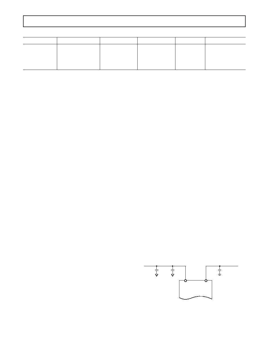
0.1 F
10 F
ANALOG
SUPPLY
DIGITAL 5V
SUPPLY
AVDD
DVDD
Figure 10. Recommended Decoupling Scheme
相关PDF资料 |
PDF描述 |
|---|---|
| VE-2NN-MX-F4 | CONVERTER MOD DC/DC 18.5V 75W |
| D38999/20WB98SA | CONN RCPT 6POS WALL MNT W/SCKT |
| PXA911/04/P | CONN PLUG 4POS W/PINS LG CABLE |
| VE-2NN-MX-F3 | CONVERTER MOD DC/DC 18.5V 75W |
| VE-B30-IV-F2 | CONVERTER MOD DC/DC 5V 150W |
相关代理商/技术参数 |
参数描述 |
|---|---|
| AD7712ARZ-REEL7 | 功能描述:IC ADC 24BIT SGNL CONDTNR 24SOIC RoHS:是 类别:集成电路 (IC) >> 数据采集 - 模数转换器 系列:- 标准包装:1 系列:- 位数:14 采样率(每秒):83k 数据接口:串行,并联 转换器数目:1 功率耗散(最大):95mW 电压电源:双 ± 工作温度:0°C ~ 70°C 安装类型:通孔 封装/外壳:28-DIP(0.600",15.24mm) 供应商设备封装:28-PDIP 包装:管件 输入数目和类型:1 个单端,双极 |
| AD7712EB | 制造商:AD 制造商全称:Analog Devices 功能描述:LC 2 MOS Signal Conditioning ADC(229.08 k) |
| AD7712SQ | 制造商:Analog Devices 功能描述: 制造商:Rochester Electronics LLC 功能描述:24 BIT SIGMA DELTA ADC IC - Bulk |
| AD7713 | 制造商:AD 制造商全称:Analog Devices 功能描述:LC2MOS Loop-Powered Signal Conditioning ADC |
发布紧急采购,3分钟左右您将得到回复。