- 您现在的位置:买卖IC网 > PDF目录10149 > AD7712ARZ-REEL (Analog Devices Inc)IC ADC 24BIT SGNL CONDTNR 24SOIC PDF资料下载
参数资料
| 型号: | AD7712ARZ-REEL |
| 厂商: | Analog Devices Inc |
| 文件页数: | 14/28页 |
| 文件大小: | 0K |
| 描述: | IC ADC 24BIT SGNL CONDTNR 24SOIC |
| 标准包装: | 1,000 |
| 位数: | 24 |
| 采样率(每秒): | 1.03k |
| 数据接口: | 串行 |
| 转换器数目: | 1 |
| 功率耗散(最大): | 45mW |
| 电压电源: | 模拟和数字,双 ± |
| 工作温度: | -40°C ~ 85°C |
| 安装类型: | 表面贴装 |
| 封装/外壳: | 24-SOIC(0.295",7.50mm 宽) |
| 供应商设备封装: | 24-SOIC W |
| 包装: | 带卷 (TR) |
| 输入数目和类型: | 1 个单端,单极;1 个差分,单极;1 个差分,双极 |
第1页第2页第3页第4页第5页第6页第7页第8页第9页第10页第11页第12页第13页当前第14页第15页第16页第17页第18页第19页第20页第21页第22页第23页第24页第25页第26页第27页第28页
REV. F
AD7712
–21–
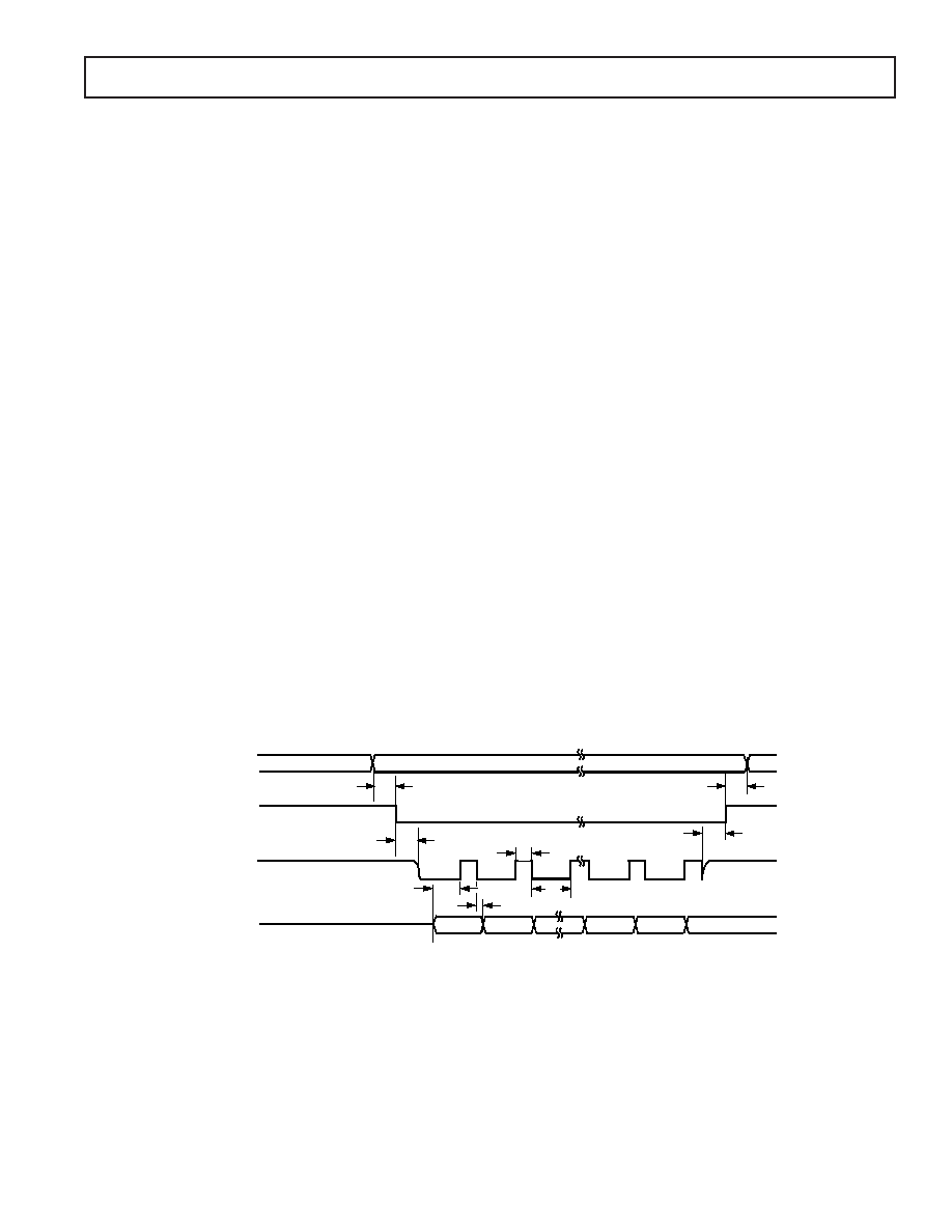
Write Operation
Data can be written to either the control register or calibration
registers. In either case, the write operation is not affected by
the
DRDY line, and the write operation does not have any
effect on the status of
DRDY. A write operation to the control
register or the calibration register must always write 24 bits to
the respective register.
Figure 12 shows a write operation to the AD7712. A0 deter-
mines whether a write operation transfers data to the control
register or to the calibration registers. This A0 signal must remain
valid for the duration of the serial write operation. The falling
edge of
TFS enables the internally generated SCLK output.
The serial data to be loaded to the AD7712 must be valid on
the rising edge of this SCLK signal. Data is clocked into the
AD7712 on the rising edge of the SCLK signal, with the MSB
transferred first. On the last active high time of SCLK, the LSB
is loaded to the AD7712. Subsequent to the next falling edge of
SCLK, the SCLK output is turned off. (The timing diagram of
Figure 12 assumes a pull-up resistor on the SCLK line.)
External Clocking Mode
The AD7712 is configured for its external clocking mode by
tying the MODE pin low. In this mode, SCLK of the AD7712
is configured as an input, and an external serial clock must be
provided to this SCLK pin. This external clocking mode is
designed for direct interface to systems that provide a serial
clock output that is synchronized to the serial data output,
including microcontrollers such as the 80C51, 87C51, 68HC11,
and 68HC05 and most digital signal processors.
Read Operation
As with the self-clocking mode, data can be read from either the
output register, the control register, or the calibration registers.
A0 determines whether the data read accesses data from the
control register or from the output/calibration registers. This A0
signal must remain valid for the duration of the serial read
operation. With A0 high, data is accessed from either the output
register or from the calibration registers. With A0 low, data is
accessed from the control register.
The function of the
DRDY line is dependent on only the output
update rate of the device and the reading of the output data
register.
DRDY goes low when a new data-word is available in
the output data register. It is reset high when the last bit of data
(either 16th bit or 24th bit) is read from the output register. If
data is not read from the output register, the
DRDY line will
remain low. The output register will continue to be updated at
the output update rate, but
DRDY will not indicate this. A read
from the device in this circumstance will access the most recent
word in the output register. If a new data-word becomes avail-
able to the output register while data is being read from the
output register,
DRDY will not indicate this, and the new data-
word will be lost to the user.
DRDY is not affected by reading
from the control register or the calibration register.
Data can be accessed from the output data register only when
DRDY is low. If RFS goes low while DRDY is high, no data
transfer will take place.
DRDY does not have any effect on
reading data from the control register or from the calibration
registers.
Figures 13a and 13b show timing diagrams for reading from the
AD7712 in the external clocking mode. Figure 13a shows a
situation where all the data is read from the AD7712 in one
read operation. Figure 13b shows a situation where the data is
read from the AD7712 over a number of read operations. Both
read operations show a read from the AD7712’s output data
register. Reads from the control register and calibration registers
are similar, but, in these cases, the
DRDY line is not related to
the read function. Depending on the output update rate, it can
go low at any stage in the control/calibration register read cycle
without affecting the read, and its status should be ignored. A
read operation from either the control or calibration registers
must always read 24 bits of data from the respective register.
SDATA (O)
SCLK (O)
TFS (I)
A0 (I)
MSB
LSB
t15
t16
t17
t18
t19
t14
t9
t10
Figure 12. Self-Clocking Mode, Control/Calibration Register Write Operation
相关PDF资料 |
PDF描述 |
|---|---|
| VE-2NN-MX-F4 | CONVERTER MOD DC/DC 18.5V 75W |
| D38999/20WB98SA | CONN RCPT 6POS WALL MNT W/SCKT |
| PXA911/04/P | CONN PLUG 4POS W/PINS LG CABLE |
| VE-2NN-MX-F3 | CONVERTER MOD DC/DC 18.5V 75W |
| VE-B30-IV-F2 | CONVERTER MOD DC/DC 5V 150W |
相关代理商/技术参数 |
参数描述 |
|---|---|
| AD7712ARZ-REEL7 | 功能描述:IC ADC 24BIT SGNL CONDTNR 24SOIC RoHS:是 类别:集成电路 (IC) >> 数据采集 - 模数转换器 系列:- 标准包装:1 系列:- 位数:14 采样率(每秒):83k 数据接口:串行,并联 转换器数目:1 功率耗散(最大):95mW 电压电源:双 ± 工作温度:0°C ~ 70°C 安装类型:通孔 封装/外壳:28-DIP(0.600",15.24mm) 供应商设备封装:28-PDIP 包装:管件 输入数目和类型:1 个单端,双极 |
| AD7712EB | 制造商:AD 制造商全称:Analog Devices 功能描述:LC 2 MOS Signal Conditioning ADC(229.08 k) |
| AD7712SQ | 制造商:Analog Devices 功能描述: 制造商:Rochester Electronics LLC 功能描述:24 BIT SIGMA DELTA ADC IC - Bulk |
| AD7713 | 制造商:AD 制造商全称:Analog Devices 功能描述:LC2MOS Loop-Powered Signal Conditioning ADC |
发布紧急采购,3分钟左右您将得到回复。