参数资料
| 型号: | AD9148BBPZRL |
| 厂商: | Analog Devices Inc |
| 文件页数: | 44/72页 |
| 文件大小: | 0K |
| 描述: | IC DAC 16BIT SPI/SRL 196BGA |
| 标准包装: | 1,500 |
| 系列: | TxDAC+® |
| 设置时间: | 20ns |
| 位数: | 16 |
| 数据接口: | 串行,SPI? |
| 转换器数目: | 4 |
| 电压电源: | 单电源 |
| 功率耗散(最大): | 2.67W |
| 工作温度: | -40°C ~ 85°C |
| 安装类型: | 表面贴装 |
| 封装/外壳: | 196-LFBGA 裸露焊盘 |
| 供应商设备封装: | 196-BGA |
| 包装: | 带卷 (TR) |
| 输出数目和类型: | 4 电流,单极 |
| 采样率(每秒): | 1G |
第1页第2页第3页第4页第5页第6页第7页第8页第9页第10页第11页第12页第13页第14页第15页第16页第17页第18页第19页第20页第21页第22页第23页第24页第25页第26页第27页第28页第29页第30页第31页第32页第33页第34页第35页第36页第37页第38页第39页第40页第41页第42页第43页当前第44页第45页第46页第47页第48页第49页第50页第51页第52页第53页第54页第55页第56页第57页第58页第59页第60页第61页第62页第63页第64页第65页第66页第67页第68页第69页第70页第71页第72页
Data Sheet
AD9148
Rev. B | Page 49 of 72
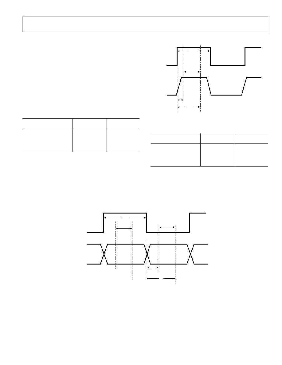
INTERFACE TIMING
The timing diagram for the digital interface port is shown in
Figure 59. The sampling point of the data bus nominally occurs
250 ps after each edge of the DCI signal and has an uncertainty of
± 250 ps when the DCI delay is set to 00b (Register 0x72[1:0]),
as illustrated by the sampling interval. The data and FRAME
signals must be valid throughout this sampling interval. The data
and FRAME signals may change at any time between sampling
intervals.
The setup (tS) and hold (tH) times with respect to the edges are
shown in Figure 59. The minimum setup and hold times are
shown in Table 16.
Table 16. Data Port Setup and Hold Times
DCI Delay
(Register 0x72, Bits[1:0])
Minimum Setup
Time, tS (ns)
Minimum Hold
Time, tH (ns)
00
0.02
0.52
01
0.16
0.78
10
0.28
1.03
11
0.36
1.16
The data interface timing can be verified by using the SED
circuitry. See the Interface Timing Validation section for details.
In data rate mode with synchronization enabled, a second timing
constraint between DCI and DACCLK must be met in addition
to the DCI-to-data timing shown in Table 17. In data rate mode,
only one FIFO slot is being used. The DCI to DACCLK timing
restriction is required to prevent data being written to and read
from the FIFO slot at the same time. The required timing
between DCI and DACCLK is shown in Figure 58.
DCI
DACCLK/
REFCLK
tDATA
tSDCI
tHDCI
SAMPLING
INTERVAL
08
91
0-
057
Figure 58. Timing Diagram for Input Data Port (Data Rate Mode with Sync On)
Table 17. DCI to DACCLK Setup and Hold Times vs. DCI
Delay Value
DCI Delay
(Register 0x72,Bits[1:0])
Minimum Setup
Time, tSDCI (ns)
Minimum Hold
Time, tHDCI (ns)
00
0.06
0.85
01
0.22
1.14
10
0.36
1.43
11
0.45
1.59
tDATA
tS
tH
SAMPLING
INTERVAL
DCI
DATA
SAMPLING
INTERVAL
08
91
0-
05
8
Figure 59. Timing Diagram for Input Data Ports
相关PDF资料 |
PDF描述 |
|---|---|
| AD9200ARS | IC ADC CMOS 10BIT 20MSPS 28-SSOP |
| AD9201ARS | IC ADC CMOS 10BIT DUAL 28-SSOP |
| AD9203ARU | IC ADC 10BIT 40MSPS 3V 28-TSSOP |
| AD9204BCPZRL7-80 | IC ADC 10BIT 80MSPS 64LFCSP |
| AD9211BCPZ-200 | IC ADC 10-BIT 200MSPS 56-LFCSP |
相关代理商/技术参数 |
参数描述 |
|---|---|
| AD9148BPCZ | 制造商:AD 制造商全称:Analog Devices 功能描述:Quad 16-Bit,1 GSPS, TxDAC+ Digital-to-Analog Converter |
| AD9148BPCZRL | 制造商:AD 制造商全称:Analog Devices 功能描述:Quad 16-Bit,1 GSPS, TxDAC+ Digital-to-Analog Converter |
| AD9148-EBZ | 功能描述:BOARD EVALUATION FOR AD9148 RoHS:是 类别:编程器,开发系统 >> 评估板 - 数模转换器 (DAC) 系列:TxDAC+® 产品培训模块:Lead (SnPb) Finish for COTS Obsolescence Mitigation Program 标准包装:1 系列:- DAC 的数量:4 位数:12 采样率(每秒):- 数据接口:串行,SPI? 设置时间:3µs DAC 型:电流/电压 工作温度:-40°C ~ 85°C 已供物品:板 已用 IC / 零件:MAX5581 |
| AD9148-M5372-EBZ | 功能描述:BOARD EVAL FOR AD9149, ADL5372 RoHS:是 类别:编程器,开发系统 >> 评估板 - 数模转换器 (DAC) 系列:* 产品培训模块:Lead (SnPb) Finish for COTS Obsolescence Mitigation Program 标准包装:1 系列:- DAC 的数量:4 位数:12 采样率(每秒):- 数据接口:串行,SPI? 设置时间:3µs DAC 型:电流/电压 工作温度:-40°C ~ 85°C 已供物品:板 已用 IC / 零件:MAX5581 |
| AD9148-M5375-EBZ | 功能描述:BOARD EVAL FOR AD9149, ADL5375 RoHS:是 类别:编程器,开发系统 >> 评估板 - 数模转换器 (DAC) 系列:* 产品培训模块:Lead (SnPb) Finish for COTS Obsolescence Mitigation Program 标准包装:1 系列:- DAC 的数量:4 位数:12 采样率(每秒):- 数据接口:串行,SPI? 设置时间:3µs DAC 型:电流/电压 工作温度:-40°C ~ 85°C 已供物品:板 已用 IC / 零件:MAX5581 |
发布紧急采购,3分钟左右您将得到回复。