参数资料
| 型号: | AD9148BBPZRL |
| 厂商: | Analog Devices Inc |
| 文件页数: | 52/72页 |
| 文件大小: | 0K |
| 描述: | IC DAC 16BIT SPI/SRL 196BGA |
| 标准包装: | 1,500 |
| 系列: | TxDAC+® |
| 设置时间: | 20ns |
| 位数: | 16 |
| 数据接口: | 串行,SPI? |
| 转换器数目: | 4 |
| 电压电源: | 单电源 |
| 功率耗散(最大): | 2.67W |
| 工作温度: | -40°C ~ 85°C |
| 安装类型: | 表面贴装 |
| 封装/外壳: | 196-LFBGA 裸露焊盘 |
| 供应商设备封装: | 196-BGA |
| 包装: | 带卷 (TR) |
| 输出数目和类型: | 4 电流,单极 |
| 采样率(每秒): | 1G |
第1页第2页第3页第4页第5页第6页第7页第8页第9页第10页第11页第12页第13页第14页第15页第16页第17页第18页第19页第20页第21页第22页第23页第24页第25页第26页第27页第28页第29页第30页第31页第32页第33页第34页第35页第36页第37页第38页第39页第40页第41页第42页第43页第44页第45页第46页第47页第48页第49页第50页第51页当前第52页第53页第54页第55页第56页第57页第58页第59页第60页第61页第62页第63页第64页第65页第66页第67页第68页第69页第70页第71页第72页
AD9148
Data Sheet
Rev. B | Page 56 of 72
CLOCK GENERATION
DAC INPUT CLOCK CONFIGURATIONS
The AD9148 DAC sample clock (DACCLK) can be sourced
directly or by clock multiplying. Clock multiplying employs
the on-chip, phased-locked loop (PLL) that accepts a reference
clock (REFCLK_x) operating at a submultiple of the desired
DACCLK rate, most commonly the data input frequency.
The PLL then multiplies the reference clock up to the desired
DACCLK frequency, which can then be used to generate all the
internal clocks required by the DAC. The clock multiplier provides
a high quality clock that meets the performance requirements of
most applications. Using the on-chip clock multiplier removes
the burden of generating and distributing the high speed DACCLK.
The second mode bypasses the clock multiplier circuitry and allows
DACCLK to be sourced directly through the CLK_x pins. This
mode enables the user to source a very high quality clock directly
to the DAC core. Sourcing the DACCLK directly through the
CLK_x pins may be necessary in demanding applications that
require the lowest possible DAC output noise, particularly at
higher output frequencies.
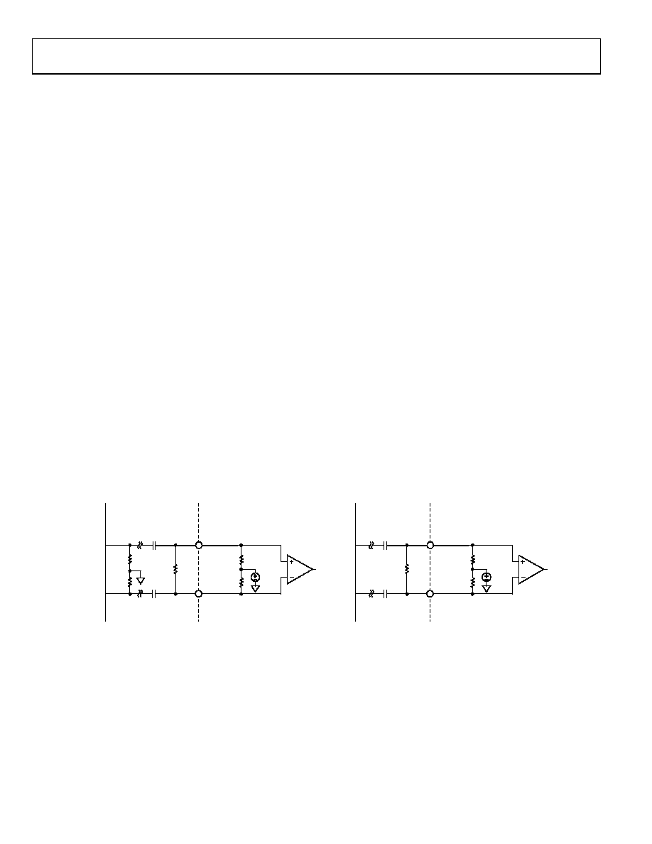
DRIVING THE CLK_x AND REFCLK_x INPUTS
The REFCLK_x and CLK_x differential inputs share similar
clock receiver input circuitry. Figure 1 shows a simplified circuit
diagram of the input, along with a recommended drive circuit.
The on-chip clock receiver has a differential input impedance of
about 10 kΩ. It is self-biased to a common-mode voltage of about
1.25 V. The recommended circuit for driving the input is a pair
of ac coupling capacitors and a differential 100 Ω termination.
The minimum input drive level to either of the clock inputs is
100 mV ppd. The optimal performance is achieved when the clock
input signal is between 500 mV ppd and 1.6 V ppd. Whether using
the on-chip clock multiplier or sourcing the DACCLK directly,
it is necessary that the input clock signal to the device have low
jitter and fast edge rates to optimize the DAC noise performance.
DIRECT CLOCKING
When a high quality, sample rate clock is connected to the AD9148,
it provides the lowest noise spectral density at the DAC outputs.
To select the differential CLK inputs as the source for the DAC
sampling clock, set the PLL enable bit to 0 (Register 0x0A, Bit 7).
Setting this bit to 0 powers down the internal PLL clock
multiplier and selects the input from the CLK_x pins as the
source for the internal DACCLK.
The device also has duty-cycle correction circuitry and differential
input level correction circuitry. Enabling these circuits may provide
improved performance in some cases. The control bits for these
functions can be found in Register 0x08.
200
100
5k
1000pF
1.25V
CLK_N/
REFCLK_N
CLK_P/
REFCLK_P
LVPECL
DRIVER
DAC
100
5k
1000pF
1.25V
CLK_N/
REFCLK_N
CLK_P/
REFCLK_P
LVDS
DRIVER
08
91
0-
071
Figure 73. Clock Receiver Circuitry and Recommended Drive Circuitry using LVPECL (Left) and LVDS (Right)
相关PDF资料 |
PDF描述 |
|---|---|
| AD9200ARS | IC ADC CMOS 10BIT 20MSPS 28-SSOP |
| AD9201ARS | IC ADC CMOS 10BIT DUAL 28-SSOP |
| AD9203ARU | IC ADC 10BIT 40MSPS 3V 28-TSSOP |
| AD9204BCPZRL7-80 | IC ADC 10BIT 80MSPS 64LFCSP |
| AD9211BCPZ-200 | IC ADC 10-BIT 200MSPS 56-LFCSP |
相关代理商/技术参数 |
参数描述 |
|---|---|
| AD9148BPCZ | 制造商:AD 制造商全称:Analog Devices 功能描述:Quad 16-Bit,1 GSPS, TxDAC+ Digital-to-Analog Converter |
| AD9148BPCZRL | 制造商:AD 制造商全称:Analog Devices 功能描述:Quad 16-Bit,1 GSPS, TxDAC+ Digital-to-Analog Converter |
| AD9148-EBZ | 功能描述:BOARD EVALUATION FOR AD9148 RoHS:是 类别:编程器,开发系统 >> 评估板 - 数模转换器 (DAC) 系列:TxDAC+® 产品培训模块:Lead (SnPb) Finish for COTS Obsolescence Mitigation Program 标准包装:1 系列:- DAC 的数量:4 位数:12 采样率(每秒):- 数据接口:串行,SPI? 设置时间:3µs DAC 型:电流/电压 工作温度:-40°C ~ 85°C 已供物品:板 已用 IC / 零件:MAX5581 |
| AD9148-M5372-EBZ | 功能描述:BOARD EVAL FOR AD9149, ADL5372 RoHS:是 类别:编程器,开发系统 >> 评估板 - 数模转换器 (DAC) 系列:* 产品培训模块:Lead (SnPb) Finish for COTS Obsolescence Mitigation Program 标准包装:1 系列:- DAC 的数量:4 位数:12 采样率(每秒):- 数据接口:串行,SPI? 设置时间:3µs DAC 型:电流/电压 工作温度:-40°C ~ 85°C 已供物品:板 已用 IC / 零件:MAX5581 |
| AD9148-M5375-EBZ | 功能描述:BOARD EVAL FOR AD9149, ADL5375 RoHS:是 类别:编程器,开发系统 >> 评估板 - 数模转换器 (DAC) 系列:* 产品培训模块:Lead (SnPb) Finish for COTS Obsolescence Mitigation Program 标准包装:1 系列:- DAC 的数量:4 位数:12 采样率(每秒):- 数据接口:串行,SPI? 设置时间:3µs DAC 型:电流/电压 工作温度:-40°C ~ 85°C 已供物品:板 已用 IC / 零件:MAX5581 |
发布紧急采购,3分钟左右您将得到回复。