- 您现在的位置:买卖IC网 > PDF目录1986 > AD9258BCPZ-125 (Analog Devices Inc)IC ADC 14BIT 125MSPS DL 64LFCSP PDF资料下载
参数资料
| 型号: | AD9258BCPZ-125 |
| 厂商: | Analog Devices Inc |
| 文件页数: | 27/44页 |
| 文件大小: | 0K |
| 描述: | IC ADC 14BIT 125MSPS DL 64LFCSP |
| 设计资源: | High Performance, Dual Channel IF Sampling Receiver (CN0140) |
| 标准包装: | 1 |
| 位数: | 14 |
| 采样率(每秒): | 125M |
| 数据接口: | 串行 |
| 转换器数目: | 2 |
| 功率耗散(最大): | 788mW |
| 电压电源: | 模拟和数字 |
| 工作温度: | -40°C ~ 85°C |
| 安装类型: | 表面贴装 |
| 封装/外壳: | 64-VFQFN 裸露焊盘,CSP |
| 供应商设备封装: | 64-LFCSP-VQ(9x9) |
| 包装: | 托盘 |
| 输入数目和类型: | 2 个差分,单极 |
第1页第2页第3页第4页第5页第6页第7页第8页第9页第10页第11页第12页第13页第14页第15页第16页第17页第18页第19页第20页第21页第22页第23页第24页第25页第26页当前第27页第28页第29页第30页第31页第32页第33页第34页第35页第36页第37页第38页第39页第40页第41页第42页第43页第44页
AD9258
Rev. A | Page 33 of 44
As detailed in the AN-877 Application Note, Interfacing to High
Speed ADCs via SPI, the data format can be selected for offset
binary, twos complement, or gray code when using the SPI control.
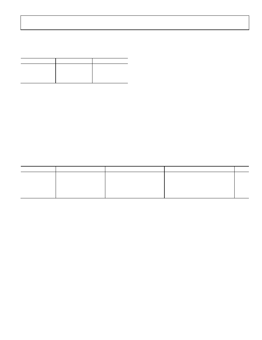
Table 12. SCLK/DFS Mode Selection (External Pin Mode)
Voltage at Pin
SCLK/DFS
SDIO/DCS
AGND
Offset binary
(default)
DCS disabled
AVDD
Twos complement
DCS enabled
(default)
Digital Output Enable Function (OEB)
The AD9258 has a flexible three-state ability for the digital output
pins. The three-state mode is enabled using the OEB pin or
through the SPI. If the OEB pin is low, the output data drivers and
DCOs are enabled. If the OEB pin is high, the output data drivers
and DCOs are placed in a high impedance state. This OEB
function is not intended for rapid access to the data bus. Note
that OEB is referenced to the digital output driver supply
(DRVDD) and should not exceed that supply voltage.
When using the SPI, the data outputs and DCO of each channel
can be independently three-stated by using the output enable
bar bit (Bit 4) in Register 0x14.
TIMING
The AD9258 provides latched data with a pipeline delay of
12 clock cycles. Data outputs are available one propagation
delay (tPD) after the rising edge of the clock signal.
The length of the output data lines and loads placed on them
should be minimized to reduce transients within the AD9258.
These transients can degrade converter dynamic performance.
The lowest typical conversion rate of the AD9258 is 10 MSPS.
At clock rates below 10 MSPS, dynamic performance can degrade.
Data Clock Output (DCO)
The AD9258 provides two data clock output (DCO) signals
intended for capturing the data in an external register. In CMOS
output mode, the data outputs are valid on the rising edge of DCO,
unless the DCO clock polarity has been changed via the SPI. In
LVDS output mode, the DCO and data output switching edges
are closely aligned. Additional delay can be added to the DCO
output using SPI Register 0x17 to increase the data setup time.
In this case, the Channel A output data is valid on the rising
edge of DCO, and the Channel B output data is valid on the
falling edge of DCO. See Figure 2, Figure 3, and Figure 4 for
a graphical timing description of the output modes.
Table 13. Output Data Format
Input (V)
Condition (V)
Offset Binary Output Mode
Twos Complement Mode
OR
VIN+ VIN
< VREF 0.5 LSB
00 0000 0000 0000
10 0000 0000 0000
1
VIN+ VIN
= VREF
00 0000 0000 0000
10 0000 0000 0000
0
VIN+ VIN
= 0
10 0000 0000 0000
00 0000 0000 0000
0
VIN+ VIN
= +VREF 1.0 LSB
11 1111 1111 1111
01 1111 1111 1111
0
VIN+ VIN
> +VREF 0.5 LSB
11 1111 1111 1111
01 1111 1111 1111
1
相关PDF资料 |
PDF描述 |
|---|---|
| AD9259ABCPZRL7-50 | IC ADC 14BIT SRL 50MSPS 48LFCSP |
| AD9260ASZRL | IC ADC 16BIT 2.5MHZ 44MQFP |
| AD9262BCPZ-10 | IC ADC 16BIT 10MHZ 64LFCSP |
| AD9266BCPZRL7-20 | IC ADC 16BIT 20MSPS 32LFCSP |
| AD9269BCPZRL7-20 | IC ADC 16BIT 20MSPS DL 64LFCSP |
相关代理商/技术参数 |
参数描述 |
|---|---|
| AD9258BCPZ-1251 | 制造商:AD 制造商全称:Analog Devices 功能描述:14-Bit, 80 MSPS/105 MSPS/125 MSPS, 1.8 V Dual Analog-to-Digital Converter (ADC) |
| AD9258BCPZ-80 | 功能描述:模数转换器 - ADC Dual 14 bit 80 high SNR ADC RoHS:否 制造商:Analog Devices 通道数量: 结构: 转换速率: 分辨率: 输入类型: 信噪比: 接口类型: 工作电源电压: 最大工作温度: 安装风格: 封装 / 箱体: |
| AD9258BCPZ-801 | 制造商:AD 制造商全称:Analog Devices 功能描述:14-Bit, 80 MSPS/105 MSPS/125 MSPS, 1.8 V Dual Analog-to-Digital Converter (ADC) |
| AD9258BCPZRL7-105 | 功能描述:模数转换器 - ADC Dual 14 bit 105 highSNR ADC RoHS:否 制造商:Analog Devices 通道数量: 结构: 转换速率: 分辨率: 输入类型: 信噪比: 接口类型: 工作电源电压: 最大工作温度: 安装风格: 封装 / 箱体: |
| AD9258BCPZRL7-1051 | 制造商:AD 制造商全称:Analog Devices 功能描述:14-Bit, 80 MSPS/105 MSPS/125 MSPS, 1.8 V Dual Analog-to-Digital Converter (ADC) |
发布紧急采购,3分钟左右您将得到回复。