- 您现在的位置:买卖IC网 > PDF目录16854 > AD9522-0/PCBZ (Analog Devices Inc)BOARD EVAL FOR AD9522-0 CLK GEN PDF资料下载
参数资料
| 型号: | AD9522-0/PCBZ |
| 厂商: | Analog Devices Inc |
| 文件页数: | 29/84页 |
| 文件大小: | 0K |
| 描述: | BOARD EVAL FOR AD9522-0 CLK GEN |
| 设计资源: | AD9522 Eval Board Schematic AD9522 BOM |
| 标准包装: | 1 |
| 主要目的: | 计时,时钟发生器 |
| 嵌入式: | 否 |
| 已用 IC / 零件: | AD9522-0 |
| 主要属性: | 12 LVDS/24 CMOS 输出,2.8 GHz VCO |
| 次要属性: | I²C & SPI 接口 |
| 已供物品: | 板 |
第1页第2页第3页第4页第5页第6页第7页第8页第9页第10页第11页第12页第13页第14页第15页第16页第17页第18页第19页第20页第21页第22页第23页第24页第25页第26页第27页第28页当前第29页第30页第31页第32页第33页第34页第35页第36页第37页第38页第39页第40页第41页第42页第43页第44页第45页第46页第47页第48页第49页第50页第51页第52页第53页第54页第55页第56页第57页第58页第59页第60页第61页第62页第63页第64页第65页第66页第67页第68页第69页第70页第71页第72页第73页第74页第75页第76页第77页第78页第79页第80页第81页第82页第83页第84页
AD9522-0
Rev. 0 | Page 35 of 84
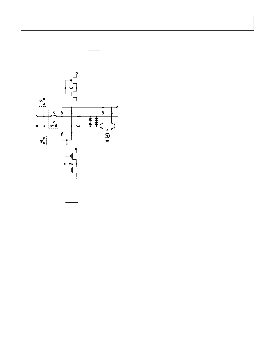
In differential mode, the reference input pins are internally self-
biased so that they can be ac-coupled via capacitors. It is possible to
dc couple to these inputs. If the differential REFIN is driven by
a single-ended signal, the unused side (REFIN) should be
decoupled via a suitable capacitor to a quiet ground.
shows the equivalent circuit of REFIN.
VS
REF1
REF2
REFIN
150
10k
12k
10k
REFIN
85k
VS
85k
VS
07
21
9-
0
66
Figure 43. REFIN Equivalent Circuit for Non-XTAL Mode
Crystal mode is nearly identical to differential mode. The user
enables a maintaining amplifier by setting the enable XTAL
OSC bit, and putting a series resonant, AT fundamental cut
crystal across the REFIN/REFIN pins.
Reference Switchover
The AD9522 supports dual single-ended CMOS inputs, as well
as a single differential reference input. In the dual single-ended
reference mode, the AD9522 supports automatic and manual
PLL reference clock switching between REF1 (on Pin REFIN)
and REF2 (on Pin REFIN). This feature supports networking
and other applications that require redundant references.
The AD9522 features a dc offset option in single-ended mode.
This option is designed to eliminate the risk of the reference
inputs chattering when they are ac-coupled and the reference
clock disappears. When using the reference switchover, the single-
ended reference inputs should be dc-coupled CMOS levels (with
the AD9522 dc offset feature disabled). Alternatively, the inputs
can be ac-coupled and dc offset feature enabled. The user should
keep in mind, however, that the minimum input amplitude for
the reference inputs is greater when the dc offset is turned on.
There are several configurable modes of reference switchover.
The switchover can be performed manually or automatically.
Manual switchover is performed either through Register 0x01C
or by using the REF_SEL pin. The automatic switchover occurs
when REF1 disappears. There is also a switchover deglitch feature,
that ensures that the PLL does not receive rising edges that are far
out of alignment with the newly selected reference.
There are two automatic reference switchover modes (0x01C):
Prefer REF1. Switch from REF1 to REF2 when REF1
disappears. Return to REF1 from REF2 when REF1 returns.
Stay on REF2. Automatically switch to REF2 if REF1
disappears, but do not switch back to REF1 if it reappears.
The reference can be set back to REF1 manually at an
appropriate time.
In automatic mode, REF1 is monitored by REF2. If REF1
disappears (two consecutive falling edges of REF2 without an
edge transition on REF1), REF1 is considered missing. On the
next subsequent rising edge of REF2, REF2 is used as the reference
clock to the PLL. If 0x01C[3] = 0b (default), when REF1 returns
(four rising edges of REF1 without two falling edges of REF2
between the REF1 edges), the PLL reference switches back to
REF1. If 0x01C[3] = 1b, the user can control when to switch
back to REF1. This is done by programming the part to manual
reference select mode (0x01C[4] = 0b) and by ensuring that the
registers and/or the REF_SEL pin is set to select the desired
reference. Automatic mode can be reenabled when REF1 is
reselected.
Manual switchover requires the presence of a clock on the reference
input that is being switched to or that the deglitching feature be
disabled (0x01C[7]).
Reference Divider R
The reference inputs are routed to the reference divider, R. R (a
14-bit counter) can be set to any value from 0 to 16,383 by writing
to 0x011 and 0x012. (Both R = 0 and R = 1 give divide-by-1.) The
output of the R divider goes to one of the PFD inputs to be
compared with the VCO frequency divided by the N divider.
The frequency applied to the PFD must not exceed the maximum
allowable frequency, which depends on the antibacklash pulse
setting (see Table 2).
The R divider has its own reset. The R divider can be reset using
the shared reset bit of the R, A, and B counters. It can also be
reset by a SYNC operation.
VCO/VCXO Feedback Divider N: P, A, B, R
The N divider is a combination of a prescaler (P) and two counters,
A and B. The total divider value is
N = (P × B) + A
where P can be 2, 4, 8, 16, or 32.
相关PDF资料 |
PDF描述 |
|---|---|
| EBM22DCMT-S288 | CONN EDGECARD 44POS .156 EXTEND |
| RNF-100-MINI-SPL-3/64-BK | HEATSHRINK RNF-100 3/64"X100'BLK |
| V110B36E150B3 | CONVERTER MOD DC/DC 36V 150W |
| RNF-100-MINI-SPL-1/16-BK | HEATSHRINK RNF-100 1/16"X75'BLK |
| H4PXS-2036G | DIP CABLE - HDP20S/AE20G/X |
相关代理商/技术参数 |
参数描述 |
|---|---|
| AD9522-1 | 制造商:AD 制造商全称:Analog Devices 功能描述:12 LVDS/24 CMOS Output Clock Generator with Integrated 2.4 GHz VCO |
| AD9522-1/PCBZ | 功能描述:BOARD EVAL FOR AD9522-1 CLK GEN RoHS:是 类别:编程器,开发系统 >> 评估演示板和套件 系列:- 标准包装:1 系列:- 主要目的:电信,线路接口单元(LIU) 嵌入式:- 已用 IC / 零件:IDT82V2081 主要属性:T1/J1/E1 LIU 次要属性:- 已供物品:板,电源,线缆,CD 其它名称:82EBV2081 |
| AD9522-1BCPZ | 功能描述:IC CLOCK GEN 2.5GHZ VCO 64LFCSP RoHS:是 类别:集成电路 (IC) >> 时钟/计时 - 时钟发生器,PLL,频率合成器 系列:- 标准包装:1,000 系列:Precision Edge® 类型:时钟/频率合成器 PLL:无 输入:CML,PECL 输出:CML 电路数:1 比率 - 输入:输出:2:1 差分 - 输入:输出:是/是 频率 - 最大:10.7GHz 除法器/乘法器:无/无 电源电压:2.375 V ~ 3.6 V 工作温度:-40°C ~ 85°C 安装类型:表面贴装 封装/外壳:16-VFQFN 裸露焊盘,16-MLF? 供应商设备封装:16-MLF?(3x3) 包装:带卷 (TR) 其它名称:SY58052UMGTRSY58052UMGTR-ND |
| AD9522-1BCPZ-REEL7 | 功能描述:IC CLOCK GEN 2.5GHZ VCO 64LFCSP RoHS:是 类别:集成电路 (IC) >> 时钟/计时 - 时钟发生器,PLL,频率合成器 系列:- 标准包装:2,000 系列:- 类型:PLL 时钟发生器 PLL:带旁路 输入:LVCMOS,LVPECL 输出:LVCMOS 电路数:1 比率 - 输入:输出:2:11 差分 - 输入:输出:是/无 频率 - 最大:240MHz 除法器/乘法器:是/无 电源电压:3.135 V ~ 3.465 V 工作温度:0°C ~ 70°C 安装类型:表面贴装 封装/外壳:32-LQFP 供应商设备封装:32-TQFP(7x7) 包装:带卷 (TR) |
| AD9522-2 | 制造商:AD 制造商全称:Analog Devices 功能描述:12 LVDS/24 CMOS Output Clock Generator with Integrated 2.2 GHz VCO |
发布紧急采购,3分钟左右您将得到回复。