- 您现在的位置:买卖IC网 > PDF目录16854 > AD9522-0/PCBZ (Analog Devices Inc)BOARD EVAL FOR AD9522-0 CLK GEN PDF资料下载
参数资料
| 型号: | AD9522-0/PCBZ |
| 厂商: | Analog Devices Inc |
| 文件页数: | 47/84页 |
| 文件大小: | 0K |
| 描述: | BOARD EVAL FOR AD9522-0 CLK GEN |
| 设计资源: | AD9522 Eval Board Schematic AD9522 BOM |
| 标准包装: | 1 |
| 主要目的: | 计时,时钟发生器 |
| 嵌入式: | 否 |
| 已用 IC / 零件: | AD9522-0 |
| 主要属性: | 12 LVDS/24 CMOS 输出,2.8 GHz VCO |
| 次要属性: | I²C & SPI 接口 |
| 已供物品: | 板 |
第1页第2页第3页第4页第5页第6页第7页第8页第9页第10页第11页第12页第13页第14页第15页第16页第17页第18页第19页第20页第21页第22页第23页第24页第25页第26页第27页第28页第29页第30页第31页第32页第33页第34页第35页第36页第37页第38页第39页第40页第41页第42页第43页第44页第45页第46页当前第47页第48页第49页第50页第51页第52页第53页第54页第55页第56页第57页第58页第59页第60页第61页第62页第63页第64页第65页第66页第67页第68页第69页第70页第71页第72页第73页第74页第75页第76页第77页第78页第79页第80页第81页第82页第83页第84页
AD9522-0
Rev. 0 | Page 51 of 84
SDA
MSB
ACKNOWLEDGE FROM
SLAVE-RECEIVER
ACKNOWLEDGE FROM
SLAVE-RECEIVER
SCL
S
P
1
2
8
9
1
2
8
3 TO 7
9
10
07
21
9-
16
2
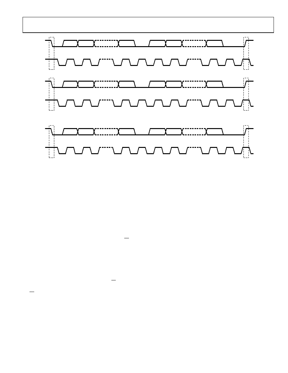
Figure 58. Acknowledge Bit
SDA
MSB = 0
ACKNOWLEDGE FROM
SLAVE-RECEIVER
ACKNOWLEDGE FROM
SLAVE-RECEIVER
SCL
S
P
1
2
8
9
1
2
8
3 TO 7
9
10
07
21
9-
16
3
Figure 59. Data Transfer Process (Master Write Mode, 2-Byte Transfer Used for Illustration)
SDA
ACKNOWLEDGE FROM
MASTER-RECEIVER
NO ACKNOWLEDGE
FROM
SLAVE-RECEIVER
SCL
S
P
1
2
8
9
1
2
8
3 TO 7
9
10
MSB = 1
0
721
9-
1
64
Figure 60. Data Transfer Process (Master Read Mode, 2-Byte Transfer Used for Illustration)
The no acknowledge bit is the ninth bit attached to any 8-bit
data byte. A no acknowledge bit is always generated by the
receiving device (receiver) to inform the transmitter that the
byte has not been received. It is done by leaving the SDA line
high during the ninth clock pulse after each 8-bit data byte.
Data Transfer Process
The master initiates data transfer by asserting a start condition.
This indicates that a data stream follows. All I2C slave devices
connected to the serial bus respond to the start condition.
The master then sends an 8-bit address byte over the SDA line,
consisting of a 7-bit slave address (MSB first) plus an R/W bit.
This bit determines the direction of the data transfer, that is,
whether data is written to or read from the slave device
(0 = write, 1 = read).
The peripheral whose address corresponds to the transmitted
address responds by sending an acknowledge bit. All other
devices on the bus remain idle while the selected device waits
for data to be read from or written to it. If the R/W bit is 0, the
master (transmitter) writes to the slave device (receiver). If the
R/W bit is 1, the master (receiver) reads from the slave device
(transmitter).
The format for these commands is described in the Data
Transfer Format section.
Data is then sent over the serial bus in the format of nine clock
pulses, one data byte (8-bit) from either master (write mode) or
slave (read mode) followed by an acknowledge bit from the
receiving device. The number of bytes that can be transmitted per
transfer is unrestricted. In write mode, the first two data bytes
immediately after the slave address byte are the internal memory
(control registers) address bytes with the high address byte first.
This addressing scheme gives a memory address up to 216 1 =
65,535. The data bytes after these two memory address bytes are
register data written into the control registers. In read mode, the
data bytes after the slave address byte are register data read from
the control registers.
When all data bytes are read or written, stop conditions are
established. In write mode, the master (transmitter) asserts a
stop condition to end data transfer during the 10th clock pulse
following the acknowledge bit for the last data byte from the
slave device (receiver). In read mode, the master device (receiver)
receives the last data byte from the slave device (transmitter)
but does not pull it low during the ninth clock pulse. This is
known as a no acknowledge bit. By receiving the no acknowledge
bit, the slave device knows that the data transfer is finished and
releases the SDA line. The master then takes the data line low
during the low period before the 10th clock pulse and high
during the 10th clock pulse to assert a stop condition.
A repeated start (Sr) condition can be used in place of a stop
condition. Furthermore, a start or stop condition can occur at
any time, and partially transferred bytes are discarded.
相关PDF资料 |
PDF描述 |
|---|---|
| EBM22DCMT-S288 | CONN EDGECARD 44POS .156 EXTEND |
| RNF-100-MINI-SPL-3/64-BK | HEATSHRINK RNF-100 3/64"X100'BLK |
| V110B36E150B3 | CONVERTER MOD DC/DC 36V 150W |
| RNF-100-MINI-SPL-1/16-BK | HEATSHRINK RNF-100 1/16"X75'BLK |
| H4PXS-2036G | DIP CABLE - HDP20S/AE20G/X |
相关代理商/技术参数 |
参数描述 |
|---|---|
| AD9522-1 | 制造商:AD 制造商全称:Analog Devices 功能描述:12 LVDS/24 CMOS Output Clock Generator with Integrated 2.4 GHz VCO |
| AD9522-1/PCBZ | 功能描述:BOARD EVAL FOR AD9522-1 CLK GEN RoHS:是 类别:编程器,开发系统 >> 评估演示板和套件 系列:- 标准包装:1 系列:- 主要目的:电信,线路接口单元(LIU) 嵌入式:- 已用 IC / 零件:IDT82V2081 主要属性:T1/J1/E1 LIU 次要属性:- 已供物品:板,电源,线缆,CD 其它名称:82EBV2081 |
| AD9522-1BCPZ | 功能描述:IC CLOCK GEN 2.5GHZ VCO 64LFCSP RoHS:是 类别:集成电路 (IC) >> 时钟/计时 - 时钟发生器,PLL,频率合成器 系列:- 标准包装:1,000 系列:Precision Edge® 类型:时钟/频率合成器 PLL:无 输入:CML,PECL 输出:CML 电路数:1 比率 - 输入:输出:2:1 差分 - 输入:输出:是/是 频率 - 最大:10.7GHz 除法器/乘法器:无/无 电源电压:2.375 V ~ 3.6 V 工作温度:-40°C ~ 85°C 安装类型:表面贴装 封装/外壳:16-VFQFN 裸露焊盘,16-MLF? 供应商设备封装:16-MLF?(3x3) 包装:带卷 (TR) 其它名称:SY58052UMGTRSY58052UMGTR-ND |
| AD9522-1BCPZ-REEL7 | 功能描述:IC CLOCK GEN 2.5GHZ VCO 64LFCSP RoHS:是 类别:集成电路 (IC) >> 时钟/计时 - 时钟发生器,PLL,频率合成器 系列:- 标准包装:2,000 系列:- 类型:PLL 时钟发生器 PLL:带旁路 输入:LVCMOS,LVPECL 输出:LVCMOS 电路数:1 比率 - 输入:输出:2:11 差分 - 输入:输出:是/无 频率 - 最大:240MHz 除法器/乘法器:是/无 电源电压:3.135 V ~ 3.465 V 工作温度:0°C ~ 70°C 安装类型:表面贴装 封装/外壳:32-LQFP 供应商设备封装:32-TQFP(7x7) 包装:带卷 (TR) |
| AD9522-2 | 制造商:AD 制造商全称:Analog Devices 功能描述:12 LVDS/24 CMOS Output Clock Generator with Integrated 2.2 GHz VCO |
发布紧急采购,3分钟左右您将得到回复。