- 您现在的位置:买卖IC网 > PDF目录16854 > AD9522-0/PCBZ (Analog Devices Inc)BOARD EVAL FOR AD9522-0 CLK GEN PDF资料下载
参数资料
| 型号: | AD9522-0/PCBZ |
| 厂商: | Analog Devices Inc |
| 文件页数: | 79/84页 |
| 文件大小: | 0K |
| 描述: | BOARD EVAL FOR AD9522-0 CLK GEN |
| 设计资源: | AD9522 Eval Board Schematic AD9522 BOM |
| 标准包装: | 1 |
| 主要目的: | 计时,时钟发生器 |
| 嵌入式: | 否 |
| 已用 IC / 零件: | AD9522-0 |
| 主要属性: | 12 LVDS/24 CMOS 输出,2.8 GHz VCO |
| 次要属性: | I²C & SPI 接口 |
| 已供物品: | 板 |
第1页第2页第3页第4页第5页第6页第7页第8页第9页第10页第11页第12页第13页第14页第15页第16页第17页第18页第19页第20页第21页第22页第23页第24页第25页第26页第27页第28页第29页第30页第31页第32页第33页第34页第35页第36页第37页第38页第39页第40页第41页第42页第43页第44页第45页第46页第47页第48页第49页第50页第51页第52页第53页第54页第55页第56页第57页第58页第59页第60页第61页第62页第63页第64页第65页第66页第67页第68页第69页第70页第71页第72页第73页第74页第75页第76页第77页第78页当前第79页第80页第81页第82页第83页第84页
AD9522-0
Rev. 0 | Page 80 of 84
APPLICATIONS INFORMATION
FREQUENCY PLANNING USING THE AD9522
The AD9522 is a highly flexible PLL. When choosing the PLL
settings and version of the AD9522, the following guidelines
should be kept in mind.
The AD9522 has four frequency dividers: the reference (or R)
divider, the feedback (or N) divider, the VCO divider, and the
channel divider. When trying to achieve a particularly difficult
frequency divide ratio requiring a large amount of frequency
division, some of the frequency division can be done by either
the VCO divider or the channel divider, thus allowing a higher
phase detector frequency and more flexibility in choosing the
loop bandwidth.
Within the AD9522 family, lower VCO frequencies generally
result in slightly better jitter. The difference in integrated jitter
(from 12 kHz to 20 MHz offset) for the same output frequency is
usually less than 150 fs over the entire VCO frequency range
(1.4 GHz to 2.95 GHz) of the AD9522 family. If the desired
frequency plan can be achieved with a version of the AD9522
that has a lower VCO frequency, choosing the lower frequency
part results in the best phase noise and the lowest jitter. However,
choosing a higher VCO frequency can result in more flexibility
in frequency planning.
Choosing a nominal charge pump current in the middle of the
allowable range as a starting point allows the designer to increase or
decrease the charge pump current, and thus allows the designer
to fine-tune the PLL loop bandwidth in either direction.
ADIsimCLK is a powerful PLL modeling tool that can be
downloaded from www.analog.com and is a very accurate tool
for determining the optimal loop filter for a given application.
USING THE AD9522 OUTPUTS FOR ADC CLOCK
APPLICATIONS
Any high speed ADC is extremely sensitive to the quality of the
sampling clock of the AD9522. An ADC can be thought of as a
sampling mixer, and any noise, distortion, or time jitter on the
clock is combined with the desired signal at the analog-to-
digital output. Clock integrity requirements scale with the analog
input frequency and resolution, with higher analog input
frequency applications at ≥14-bit resolution being the most
stringent. The theoretical SNR of an ADC is limited by the ADC
resolution and the jitter on the sampling clock. Considering an
ideal ADC of infinite resolution where the step size and
quantization error can be ignored, the available SNR can be
expressed approximately by
π
=
J
At
f
SNR
2
1
20log
(dB)
where:
fA is the highest analog frequency being digitized.
tJ is the rms jitter on the sampling clock.
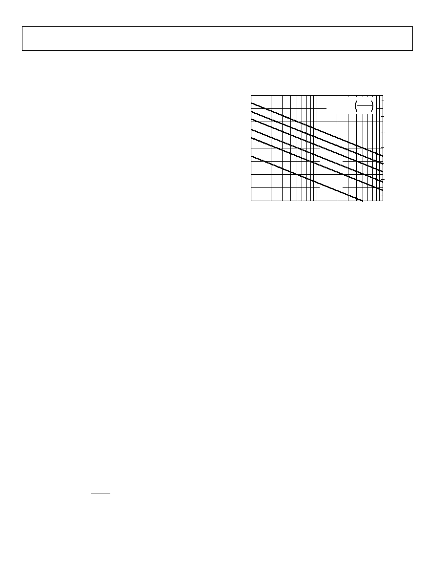
Figure 70 shows the required sampling clock jitter as a function
of the analog frequency and effective number of bits (ENOB).
fA (MHz)
S
NR
(
d
B)
EN
O
B
10
1k
100
30
40
50
60
70
80
90
100
110
6
8
10
12
14
16
18
t
J
= 100f
s
t
J
= 200f
s
t
J
= 400f
s
t
J
= 1ps
t
J
= 2ps
t
J
= 10p
s
SNR = 20log
1
2πfAtJ
07
21
9-
04
4
Figure 70. SNR and ENOB vs. Analog Input Frequency
See the AN-756 Application Note and the AN-501 Application
Note at www.analog.com.
Many high performance ADCs feature differential clock inputs
to simplify the task of providing the required low jitter clock on
a noisy PCB. Distributing a single-ended clock on a noisy PCB
can result in coupled noise on the sampling clock. Differential
distribution has inherent common-mode rejection that can
provide superior clock performance in a noisy environment.
The differential LVDS outputs of the AD9522 enable clock
solutions that maximize converter SNR performance.
The input requirements of the ADC (differential or single-
ended, logic level termination) should be considered when
selecting the best clocking/converter solution. In some cases,
the LVPECL outputs of the AD9520 may be desirable for
clocking a converter instead of the AD9522’s LVDS outputs.
LVDS CLOCK DISTRIBUTION
The AD9522 provides clock outputs that are selectable as either
CMOS or LVDS level outputs. LVDS is a differential output
option that uses a current mode output stage. The nominal
current is 3.5 mA, which yields 350 mV output swing across a
100 Ω resistor. An output current of 7 mA is also available in
cases where a larger output swing is required. The LVDS output
meets or exceeds all ANSI/TIA/EIA-644 specifications.
相关PDF资料 |
PDF描述 |
|---|---|
| EBM22DCMT-S288 | CONN EDGECARD 44POS .156 EXTEND |
| RNF-100-MINI-SPL-3/64-BK | HEATSHRINK RNF-100 3/64"X100'BLK |
| V110B36E150B3 | CONVERTER MOD DC/DC 36V 150W |
| RNF-100-MINI-SPL-1/16-BK | HEATSHRINK RNF-100 1/16"X75'BLK |
| H4PXS-2036G | DIP CABLE - HDP20S/AE20G/X |
相关代理商/技术参数 |
参数描述 |
|---|---|
| AD9522-1 | 制造商:AD 制造商全称:Analog Devices 功能描述:12 LVDS/24 CMOS Output Clock Generator with Integrated 2.4 GHz VCO |
| AD9522-1/PCBZ | 功能描述:BOARD EVAL FOR AD9522-1 CLK GEN RoHS:是 类别:编程器,开发系统 >> 评估演示板和套件 系列:- 标准包装:1 系列:- 主要目的:电信,线路接口单元(LIU) 嵌入式:- 已用 IC / 零件:IDT82V2081 主要属性:T1/J1/E1 LIU 次要属性:- 已供物品:板,电源,线缆,CD 其它名称:82EBV2081 |
| AD9522-1BCPZ | 功能描述:IC CLOCK GEN 2.5GHZ VCO 64LFCSP RoHS:是 类别:集成电路 (IC) >> 时钟/计时 - 时钟发生器,PLL,频率合成器 系列:- 标准包装:1,000 系列:Precision Edge® 类型:时钟/频率合成器 PLL:无 输入:CML,PECL 输出:CML 电路数:1 比率 - 输入:输出:2:1 差分 - 输入:输出:是/是 频率 - 最大:10.7GHz 除法器/乘法器:无/无 电源电压:2.375 V ~ 3.6 V 工作温度:-40°C ~ 85°C 安装类型:表面贴装 封装/外壳:16-VFQFN 裸露焊盘,16-MLF? 供应商设备封装:16-MLF?(3x3) 包装:带卷 (TR) 其它名称:SY58052UMGTRSY58052UMGTR-ND |
| AD9522-1BCPZ-REEL7 | 功能描述:IC CLOCK GEN 2.5GHZ VCO 64LFCSP RoHS:是 类别:集成电路 (IC) >> 时钟/计时 - 时钟发生器,PLL,频率合成器 系列:- 标准包装:2,000 系列:- 类型:PLL 时钟发生器 PLL:带旁路 输入:LVCMOS,LVPECL 输出:LVCMOS 电路数:1 比率 - 输入:输出:2:11 差分 - 输入:输出:是/无 频率 - 最大:240MHz 除法器/乘法器:是/无 电源电压:3.135 V ~ 3.465 V 工作温度:0°C ~ 70°C 安装类型:表面贴装 封装/外壳:32-LQFP 供应商设备封装:32-TQFP(7x7) 包装:带卷 (TR) |
| AD9522-2 | 制造商:AD 制造商全称:Analog Devices 功能描述:12 LVDS/24 CMOS Output Clock Generator with Integrated 2.2 GHz VCO |
发布紧急采购,3分钟左右您将得到回复。