- 您现在的位置:买卖IC网 > PDF目录11768 > AD9981KSTZ-80 (Analog Devices Inc)IC INTERFACE 10BIT ANALOG 80LQFP PDF资料下载
参数资料
| 型号: | AD9981KSTZ-80 |
| 厂商: | Analog Devices Inc |
| 文件页数: | 35/44页 |
| 文件大小: | 0K |
| 描述: | IC INTERFACE 10BIT ANALOG 80LQFP |
| 标准包装: | 90 |
| 应用: | 视频 |
| 接口: | 模拟 |
| 电源电压: | 3.13 V ~ 3.47 V |
| 封装/外壳: | 80-LQFP |
| 供应商设备封装: | 80-LQFP(14x14) |
| 包装: | 管件 |
| 安装类型: | 表面贴装 |
第1页第2页第3页第4页第5页第6页第7页第8页第9页第10页第11页第12页第13页第14页第15页第16页第17页第18页第19页第20页第21页第22页第23页第24页第25页第26页第27页第28页第29页第30页第31页第32页第33页第34页当前第35页第36页第37页第38页第39页第40页第41页第42页第43页第44页
AD9981
Preliminary Technical Data
Rev. 0 | Page 40 of 44
TWO-WIRE SERIAL CONTROL PORT
A two-wire serial interface control interface is provided. Up to
two AD9981 devices may be connected to the two-wire serial
interface, with each device having a unique address.
The two-wire serial interface comprises a clock (SCL) and a bi-
directional data (SDA) pin. The analog flat panel interface acts
as a slave for receiving and transmitting data over the serial
interface. When the serial interface is not active, the logic levels
on SCL and SDA are pulled high by external pull-up resistors.
Data received or transmitted on the SDA line must be stable for
the duration of the positive-going SCL pulse. Data on SDA must
change only when SCL is low. If SDA changes state while SCL is
high, the serial interface interprets that action as a start or stop
sequence.
The following are the five components to serial bus operation:
Start signal
Slave address byte
Base register address byte
Data byte to read or write
Stop signal
When the serial interface is inactive (SCL and SDA are high),
communications are initiated by sending a start signal. The start
signal is a high-to-low transition on SDA while SCL is high.
This signal alerts all slaved devices that a data transfer sequence
is coming.
The first eight bits of data transferred after a start signal
comprise a 7-bit slave address (the first seven bits) and a single
R/W\ bit (the eighth bit). The R/W\ bit indicates the direction
of data transfer, read from 1 or write to 0 on the slave device. If
the transmitted slave address matches the address of the device
(set by the state of the Serial A0 address [SA0] input pin in
Table 70), the AD9981 acknowledges the match by bringing
SDA low on the 9th SCL pulse. If the addresses do not match,
the AD9981 does not acknowledge it.
Table 70. Serial Port Addresses
Bit 7
Bit 6
Bit 5
Bit 4
Bit 3
Bit 2
Bit 1
A6 (MSB)
A5
A4
A3
A2
A1
A0
1
0
1
0
1
0
1
0
1
DATA TRANSFER VIA SERIAL INTERFACE
For each byte of data read or written, the MSB is the first bit in
the sequence.
If the AD9981 does not acknowledge the master device during a
write sequence, the SDA remains high so the master can gener-
ate a stop signal. If the master device does not acknowledge the
AD9981 during a read sequence, the AD9981 interprets this as
end-of-data. The SDA remains high so the master can generate
a stop signal.
Writing data to specific control registers of the AD9981 requires
that the 8-bit address of the control register of interest be writ-
ten after the slave address has been established. This control
register address is the base address for subsequent write opera-
tions. The base address auto-increments by one for each byte of
data written after the data byte intended for the base address. If
more bytes are transferred than there are available addresses,
the address will not increment and remain at its maximum
value of 0x2E. Any base address higher than 0x2E will not pro-
duce an acknowledge signal. Data are read from the control
registers of the AD9981 in a similar manner. Reading requires
two data transfer operations:
The base address must be written with the R/W bit of the slave
address byte low to set up a sequential read operation. Reading
(the R/W\ bit of the slave address byte high) begins at the
previously established base address. The address of the read
register auto-increments after each byte is transferred.
To terminate a read/write sequence to the AD9981, a stop signal
must be sent. A stop signal comprises a low-to-high transition
of SDA while SCL is high.
A repeated start signal occurs when the master device driving
the serial interface generates a start signal without first genera-
ting a stop signal to terminate the current communication. This
is used to change the mode of communication (read, write)
between the slave and master without releasing the serial
interface lines.
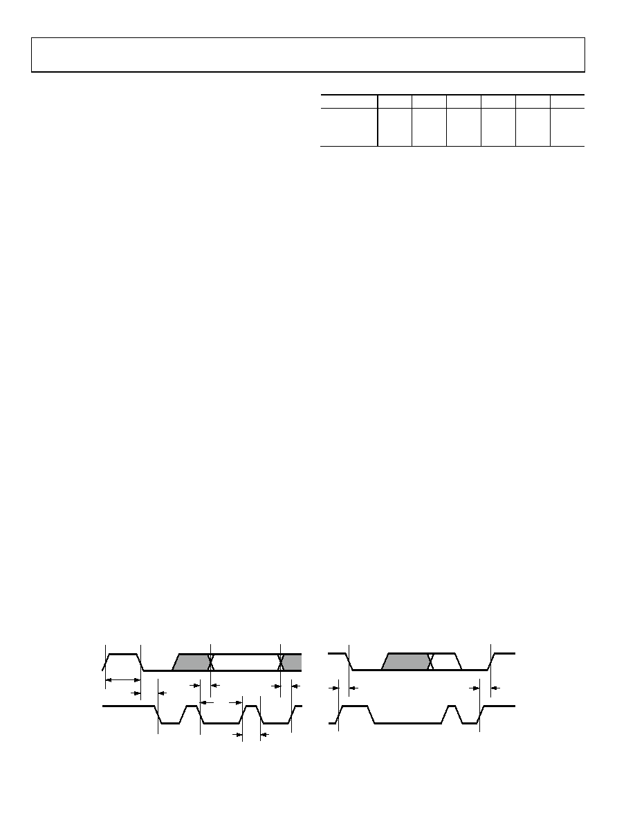
SDA
SCL
tBUFF
tSTAH
tDHO
tDSU
tDAL
tDAH
tSTASU
tSTOSU
04739-011
Figure 17. Serial Port Read/Write Timing
相关PDF资料 |
PDF描述 |
|---|---|
| PIC16LF1906-I/MV | MCU PIC 512B FLASH XLP 28-UQFN |
| VI-B41-IX-F1 | CONVERTER MOD DC/DC 12V 75W |
| MS27505E21B39P | CONN RCPT 39POS BOX MNT W/PINS |
| PIC16F721-I/P | MCU PIC 4K FLASH 20-DIP |
| 5227079-6 | CONN PLUG BNC RG55,223 CRIMP AU |
相关代理商/技术参数 |
参数描述 |
|---|---|
| AD9981KSTZ-95 | 功能描述:IC INTERFACE 10BIT ANALOG 80LQFP RoHS:是 类别:集成电路 (IC) >> 接口 - 专用 系列:- 特色产品:NXP - I2C Interface 标准包装:1 系列:- 应用:2 通道 I²C 多路复用器 接口:I²C,SM 总线 电源电压:2.3 V ~ 5.5 V 封装/外壳:16-TSSOP(0.173",4.40mm 宽) 供应商设备封装:16-TSSOP 包装:剪切带 (CT) 安装类型:表面贴装 产品目录页面:825 (CN2011-ZH PDF) 其它名称:568-1854-1 |
| AD9981XSTZ-110 | 制造商:Analog Devices 功能描述:HIGH PERFORMANCE 10-BIT DISPLAY INTERFACE - Bulk |
| AD9983A | 制造商:AD 制造商全称:Analog Devices 功能描述:High Performance 8-Bit Display Interface |
| AD9983A/PCB | 制造商:AD 制造商全称:Analog Devices 功能描述:High Performance 8-Bit Display Interface |
| AD9983A/PCBZ | 功能描述:KIT EVALUATION AD9983A RoHS:是 类别:编程器,开发系统 >> 评估演示板和套件 系列:Advantiv® 标准包装:1 系列:PCI Express® (PCIe) 主要目的:接口,收发器,PCI Express 嵌入式:- 已用 IC / 零件:DS80PCI800 主要属性:- 次要属性:- 已供物品:板 |
发布紧急采购,3分钟左右您将得到回复。