参数资料
| 型号: | AD9995KCPZ |
| 厂商: | Analog Devices Inc |
| 文件页数: | 11/60页 |
| 文件大小: | 0K |
| 描述: | IC CCD SIGNAL PROCESSOR 56-LFCSP |
| 标准包装: | 1 |
| 类型: | CCD 信号处理器,12 位 |
| 输入类型: | 逻辑 |
| 输出类型: | 逻辑 |
| 接口: | 3 线串口 |
| 电流 - 电源: | 30mA |
| 安装类型: | 表面贴装 |
| 封装/外壳: | 56-VFQFN 裸露焊盘,CSP |
| 供应商设备封装: | 56-LFCSP-VQ(8x8) |
| 包装: | 托盘 |
第1页第2页第3页第4页第5页第6页第7页第8页第9页第10页当前第11页第12页第13页第14页第15页第16页第17页第18页第19页第20页第21页第22页第23页第24页第25页第26页第27页第28页第29页第30页第31页第32页第33页第34页第35页第36页第37页第38页第39页第40页第41页第42页第43页第44页第45页第46页第47页第48页第49页第50页第51页第52页第53页第54页第55页第56页第57页第58页第59页第60页
AD9995
–19–
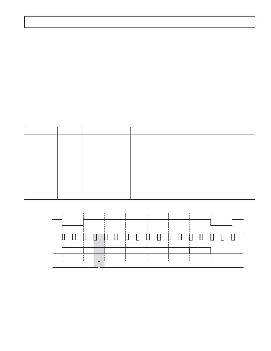
Complete Field: Combining V-Sequences
After the V-sequences have been created, they are combined to
create different readout fields. A field consists of up to seven
different regions, and within each region a different V-sequence
can be selected. Figure 18 shows how the sequence change posi-
tions (SCP) designate the line boundary for each region, and
the VSEQSEL registers then select which V-sequence is used
during each region. Registers to control the VSG outputs are also
included in the Field registers.
Table VII summarizes the registers used to create the different
fields. Up to six different fields can be preprogrammed using all
of the Field registers.
The VEQSEL registers, one for each region, select which of the
10 V-sequences will be active during each region.The SWEEP
registers are used to enable SWEEP mode during any region.
The MULTI registers are used to enable Multiplier mode dur-
ing any region.The SCP registers create the line boundaries for
each region.The VDLEN register specifies the total number of
lines in the field.The total number of pixels per line (HDLEN) is
specified in the V-sequence registers, but the HDLAST register
specifies the number of pixels in the last line of the field.The
VPATSECOND register is used to add a second V-pattern group
to the V1–6 outputs during the sensor gate (VSG) line.
The SGMASK register is used to enable or disable each indi-
vidual VSG output.There is a single bit for each VSG output;
setting the bit high will mask the output, setting it low will enable
the output.The SGPAT register assigns one of the four different
SG patterns to each VSG output.The individual SG patterns are
created separately using the SG pattern registers.The SGLINE1
register specifies which line in the field will contain the VSG out-
puts.The optional SGLINE2 register allows the same VSG pulses
to be repeated on a different line.
Table VII. Field Registers
Register
Length
Range
Description
VSEQSEL
4b
0–9 V-Sequence #
Selected V-Sequence for Each Region in the Field.
SWEEP
1b
High/Low
Enables Sweep Mode for Each Region,When Set High.
MULTI
1b
High/Low
Enables Multiplier Mode for Each Region,When Set High.
SCP
12b
0–4095 Line #
Sequence Change Position for Each Region.
VDLEN
12b
0–4095 # of Lines
Total Number of Lines in Each Field.
HDLAST
12b
0–4095 # of Pixels
Length in Pixels of the Last HD Line in Each Field.
VPATSECOND
4b
0–9 V-Pattern Group #
Selected V-Pattern Group for Second Pattern Applied During VSG Line.
SGMASK
6b
High/Low, Each VSG
Set High to Mask Each Individual VSG Output.VSG1 [0],VSG2 [1],
VSG3 [2],VSG4 [3],VSG5 [4].
SGPATSEL
12b
0–3 Pattern #, Each VSG
Selects the VSG Pattern Number for Each VSG Output.VSG1 [1:0],
VSG2 [3:2],VSG3 [5:4],VSG4 [7:6],VSG5 [9:8].
SGLINE1
12b
0–4095 Line #
Selects the Line in the Field where the VSG Are Active.
SGLINE2
12b
0–4095 Line #
Selects a Second Line in the Field to Repeat the VSG Signals.
VD
REGION 0
FIELD SETTINGS:
1. SEQUENCE CHANGE POSITIONS (SCP1–6) DEFINE EACH OF THE 7 REGIONS IN THE FIELD.
2. VSEQSEL0–6 SELECTS THE DESIRED V-SEQUENCE (0–9) FOR EACH REGION.
3. SGLINE1 REGISTER SELECTS WHICH HD LINE IN THE FIELD WILL CONTAIN THE SENSOR GATE PULSE(S).
V1–V6
HD
SCP 1
SCP 2
VSEQSEL0
VSEQSEL1
SCP 3
VSEQSEL2
SCP 4
VSEQSEL3
SCP 5
VSEQSEL4
SCP 6
VSEQSEL5
VSEQSEL6
REGION 1
REGION 2
REGION 3
REGION 4
REGION 5
REGION 6
VSG
SGLINE
SGLINE1
Figure 18. Complete Field Is Divided into Regions
REV. 0
OBSOLETE
相关PDF资料 |
PDF描述 |
|---|---|
| ADA4424-6ARUZ | IC FILTR VID6CH SD/ED/HD 38TSSOP |
| ADATE302-02BBCZ | IC DCL ATE 500MHZ DUAL 84CSPBGA |
| ADATE304BBCZ | IC DCL ATE 200MHZ DUAL 84CSPBGA |
| ADATE305BSVZ | IC DCL ATE 250MHZ DUAL 100TQFP |
| ADAU1328BSTZ | IC CODEC 24BIT 2ADC/8DAC 48LQFP |
相关代理商/技术参数 |
参数描述 |
|---|---|
| AD9995KCPZRL | 功能描述:IC CCD SIGNAL PROCESSOR 56-LFCSP RoHS:是 类别:集成电路 (IC) >> 接口 - 传感器和探测器接口 系列:- 其它有关文件:Automotive Product Guide 产品培训模块:Lead (SnPb) Finish for COTS Obsolescence Mitigation Program 标准包装:74 系列:- 类型:触控式传感器 输入类型:数字 输出类型:数字 接口:JTAG,串行 电流 - 电源:100µA 安装类型:表面贴装 封装/外壳:20-TSSOP(0.173",4.40mm 宽) 供应商设备封装:20-TSSOP 包装:管件 |
| AD9995KCPZRL7 | 制造商:Rochester Electronics LLC 功能描述: 制造商:Analog Devices 功能描述: |
| AD9996BBCZ | 制造商:Rochester Electronics LLC 功能描述:14B 40 MSPS AFETG CONVERTER - Bulk |
| AD9996BBCZRL | 制造商:Rochester Electronics LLC 功能描述:- Bulk |
| AD-9FT4-B2 | 制造商:Pan Pacific 功能描述: |
发布紧急采购,3分钟左右您将得到回复。