- 您现在的位置:买卖IC网 > PDF目录1776 > ADP1823ACPZ-R7 (Analog Devices Inc)IC REG CTRLR BUCK PWM VM 32LFCSP PDF资料下载
参数资料
| 型号: | ADP1823ACPZ-R7 |
| 厂商: | Analog Devices Inc |
| 文件页数: | 24/32页 |
| 文件大小: | 0K |
| 描述: | IC REG CTRLR BUCK PWM VM 32LFCSP |
| 标准包装: | 1 |
| PWM 型: | 电压模式 |
| 输出数: | 2 |
| 频率 - 最大: | 720kHz |
| 占空比: | 90% |
| 电源电压: | 3.7 V ~ 20 V |
| 降压: | 是 |
| 升压: | 无 |
| 回扫: | 无 |
| 反相: | 无 |
| 倍增器: | 无 |
| 除法器: | 无 |
| Cuk: | 无 |
| 隔离: | 无 |
| 工作温度: | -40°C ~ 125°C |
| 封装/外壳: | 32-VFQFN 裸露焊盘,CSP |
| 包装: | 标准包装 |
| 产品目录页面: | 791 (CN2011-ZH PDF) |
| 其它名称: | ADP1823ACPZ-R7DKR |
第1页第2页第3页第4页第5页第6页第7页第8页第9页第10页第11页第12页第13页第14页第15页第16页第17页第18页第19页第20页第21页第22页第23页当前第24页第25页第26页第27页第28页第29页第30页第31页第32页
�� �
�
�ADP1823�
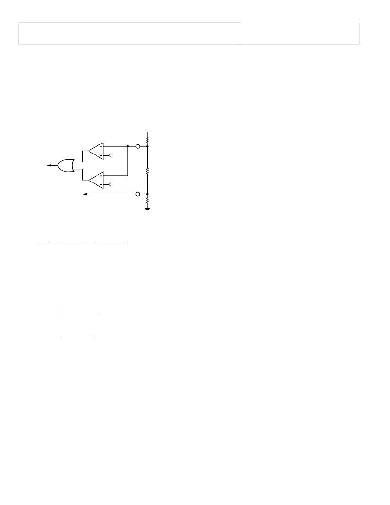
�Setting� the� Channel� 2� Undervoltage� Threshold� for�
�Ratiometric� Tracking�
�If� FB2� is� regulated� to� a� voltage� lower� than� 0.6� V� by� configuring�
�TRK2� for� ratiometric� tracking,� the� Channel� 2� undervoltage�
�threshold� can� be� set� appropriately� by� splitting� the� top� resistor�
�in� the� voltage� divider,� as� shown� in� Figure� 33.� R� BOT� is� the� same� as�
�calculated� for� the� compensation� in� Equation� 52,� and�
�THERMAL� CONSIDERATIONS�
�The� current� required� to� drive� the� external� MOSFETs� comprises�
�the� vast� majority� of� the� power� dissipation� of� the� ADP1823.� The�
�on-chip� LDO� regulates� down� to� 5� V,� and� this� 5� V� supplies� the�
�drivers.� The� full� gate� drive� current� passes� through� the� LDO� and�
�is� then� dissipated� in� the� gate� drivers.� The� power� dissipated� on�
�the� gate� drivers� on� the� ADP1823� is�
�R� TOP� =� R� A� +� R� B�
�B�
�CHANNEL� 2�
�OUTPUT�
�VOLTAGE�
�R� A�
�UV2�
�(53)�
�P� D� =� V� IN� f� SW� (� Q� DH1� +� Q� DL1� +� Q� DH2� +� Q� DL2� )�
�where:�
�V� IN� is� the� voltage� applied� to� IN.�
�f� SW� is� the� switching� frequency.�
�(57)�
�Q� numbers� are� the� total� gate� charge� specifications� from� the�
�550mV�
�selected� MOSFET� data� sheets.�
�POK2�
�R� B�
�The� power� dissipation� heats� the� ADP1823.� As� the� switching�
�frequency,� the� input� voltage,� and� the� MOSFET� size� increase,� the�
�TO� ERROR�
�AMPLIFIER�
�750mV�
�FB2�
�R� BOT�
�power� dissipation� on� the� ADP1823� increases.� Care� must� be� taken�
�not� to� exceed� the� maximum� junction� temperature.� To� calculate�
�the� junction� temperature� from� the� ambient� temperature� and�
�power� dissipation�
�Figure� 33.� Setting� the� Channel� 2� Undervoltage� Threshold�
�T� J� =� T� A� +� P� D� θ� JA�
�(58)�
�The� current� in� all� the� resistors� is� the� same.�
�The� thermal� resistance,� θ� JA� ,� of� the� package� is� typically� 40°C/W�
�V� FB� 2�
�R� BOT�
�=�
�V� UV� 2� ?� V� FB� 2�
�R� B�
�=�
�V� OUT� 2� ?� V� UV� 2�
�R� A�
�(54)�
�depending� on� board� layout,� and� the� maximum� specified� junction�
�temperature� is� 125°C,� which� means� that� at� a� maximum� ambient�
�temperature� of� 85°C� without� airflow,� the� maximum� dissipation�
�Solving� for� R� A� and� R� B� ,�
�(� V� OUTA� 2� ?� V� UV� 2� )�
�(� V� ?� V� FB� 2� )�
�R� B� =� R� BOT�
�where:�
�V� UV2� is� 600� mV.�
�V� FB2� is� the� feedback� voltage� value� set� during� the� ratiometric�
�tracking� calculations.�
�V� OUT2� is� the� Channel� 2� output� voltage.�
�B�
�R� A� =� R� BOT�
�V� FB� 2�
�UV� 2�
�V� FB� 2�
�allowed� is� about� 1� W.�
�A� thermal� shutdown� protection� circuit� on� the� ADP1823� shuts�
�off� the� LDO� and� the� controllers� if� the� die� temperature� exceeds�
�approximately� 145°C,� but� this� is� a� gross� fault� protection� only�
�and� should� not� be� relied� upon� for� system� reliability.�
�(55)�
�(56)�
�Rev.� D� |� Page� 24� of� 32�
�相关PDF资料 |
PDF描述 |
|---|---|
| ADP1828ACPZ-R7 | IC REG CTRLR BUCK PWM VM 20LFCSP |
| ADP1829ACPZ-R7 | IC REG CTRLR BUCK PWM VM 32LFCSP |
| ADP1850ACPZ-R7 | IC REG CTRLR BUCK PWM CM 32LFCSP |
| ADP1864AUJZ-R7 | IC REG CTRLR BUCK PWM TSOT23-6 |
| ADP1871ACPZ-0.6-R7 | IC REG CTRLR BUCK PWM CM 10LFCSP |
相关代理商/技术参数 |
参数描述 |
|---|---|
| ADP1823-EVAL | 功能描述:BOARD EVAL FOR ADP1823 RoHS:否 类别:编程器,开发系统 >> 评估板 - DC/DC 与 AC/DC(离线)SMPS 系列:- 标准包装:1 系列:- 主要目的:DC/DC,步降 输出及类型:1,非隔离 功率 - 输出:- 输出电压:3.3V 电流 - 输出:3A 输入电压:4.5 V ~ 28 V 稳压器拓扑结构:降压 频率 - 开关:250kHz 板类型:完全填充 已供物品:板 已用 IC / 零件:L7981 其它名称:497-12113STEVAL-ISA094V1-ND |
| ADP1828 | 制造商:AD 制造商全称:Analog Devices 功能描述:Synchronous Buck PWM, Step-Down, DC-to-DC Controller |
| ADP1828ACPZ-R7 | 功能描述:IC REG CTRLR BUCK PWM VM 20LFCSP RoHS:是 类别:集成电路 (IC) >> PMIC - 稳压器 - DC DC 切换控制器 系列:- 标准包装:2,500 系列:- PWM 型:电流模式 输出数:1 频率 - 最大:500kHz 占空比:96% 电源电压:4 V ~ 36 V 降压:无 升压:是 回扫:无 反相:无 倍增器:无 除法器:无 Cuk:无 隔离:无 工作温度:-40°C ~ 125°C 封装/外壳:24-WQFN 裸露焊盘 包装:带卷 (TR) |
| ADP1828-BL1-EVZ | 制造商:Analog Devices 功能描述:BLANK ADISIMPOWER EVAL ADP1828 - Boxed Product (Development Kits) |
| ADP1828-BL2-EVZ | 制造商:Analog Devices 功能描述:BLANK ADISIMPOWER EVAL ADP1828 - Boxed Product (Development Kits) |
发布紧急采购,3分钟左右您将得到回复。